TMS320F2837x + Spartan6/Domestic FPGA Low-Cost High-Real-Time Injection Molding Machine Motion Controller Hardware and Software Design Solution
A precise injection molding machine control system was designed using a DSP as the slave controller and an ARM as the master controller. The slave controller is responsible for executing control algorithms and I/O control, while the master controller handles the Human-Machine Interface (HMI) and mold data management. This control system offers good real-time performance and high control precision. A drawback is that control algorithms were not designed within the control system itself, making it impossible to verify compatibility with different control algorithms.
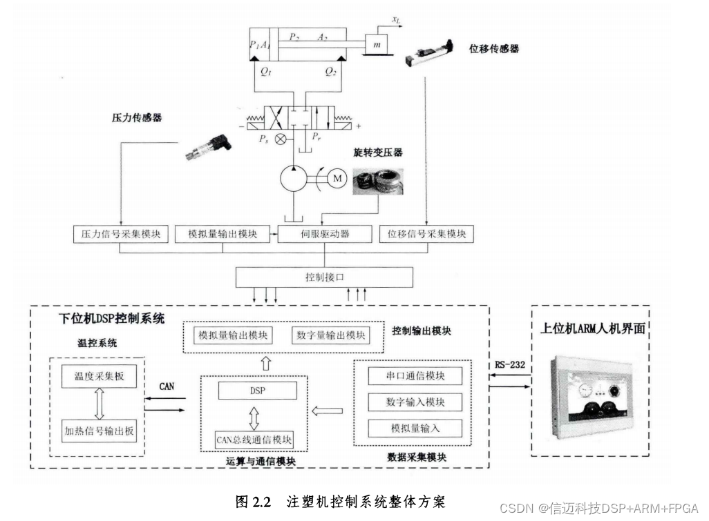
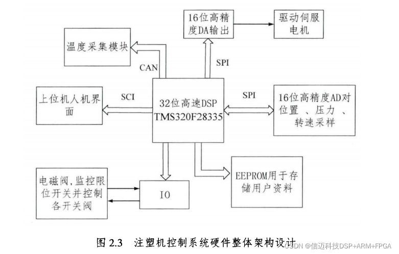
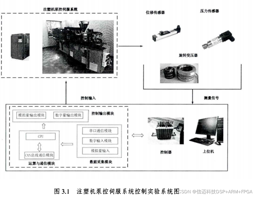
The injection molding machine controller is a control system based on TI's TMS320F28335 chip, serving as the core component of the entire injection molding machine's pump-controlled servo system. The control system can perform real-time monitoring of state information such as pressure, position, temperature, and flow rate from various parts by collecting corresponding sensor signals. It then processes these signals by executing designed control algorithms to complete the actions required by the injection molding process.
1 Evaluation Board Introduction
Ø Based on TI TMS320F2837x series single/dual-core 32-bit floating-point MCU controller + Xilinx Spartan-6 low-power FPGA;
Ø TI TMS320F2837x has a main frequency of 200MHz, integrating a single-precision floating-point unit (FPU), trigonometric math unit (TMU), complex math unit (VCA-II), and single/dual programmable control law accelerator (CLA). It includes 512K/1MByte ROM and 172K/204KByte RAM;
Ø The MCU integrates two zero-pin 10MHz oscillators, a crystal oscillator, a watchdog timer module, and a missing clock detection circuit;
Ø The FPGA chip model is XC6SLX16-2CSG324I, with 14K logic cells and 32 DSP Slices, pin-to-pin compatible with XC6SLX9/25/45-2CSG324I, offering strong platform upgrade capability;
Ø TMS320F2837x and FPGA are connected internally via I2C, uPP, EMIF, and other buses, enabling more efficient and flexible interconnection between FPGA and MCU;
Ø The development board exposes ePWM, eQEP, McBSP, ADC, and other interfaces, suitable for various industrial control equipment;
Ø The development board exposes common communication interfaces such as USB OTG, RS232, RS485, and CAN;
Ø Uses precision industrial-grade B2B connectors, occupying minimal space, offering strong stability, easy to plug and unplug, and anti-reverse insertion;
Ø Provides rich development examples, easy to get started, supports bare-metal and SYS/BIOS operating systems.
Figure 1
The XM2837xF-EVM is a high-end single/dual-core floating-point development board designed by Shenzhen Xinmai based on the SOM-XM2837xF core board. It provides users with a test platform for the SOM-XM2837xF core board, enabling quick evaluation of its overall performance.
The XM2837xF-EVM baseboard adopts a 4-layer board design with immersion gold and lead-free process. It not only provides customers with system driver source code, rich demo programs, a complete software development kit, and detailed TMS320F28x system development documentation, but also assists customers with baseboard development, offers long-term and comprehensive technical support, helping customers achieve rapid secondary development and quick product launch.
2 Typical Application Areas
- ü Power electronics control (e.g., MMC converters)
- ü Microgrid control
- ü Power acquisition
- ü Power line communication
- ü Digital power supplies
- ü Industrial drives
- ü Servo motor control
3 Hardware and Software Parameters
Figure 4 Xilinx Spartan-6 FPGA Feature Parameters
3.1 Hardware Parameters
Table 1 MCU-side Hardware Parameters
CPU
TI dual-core TMS320F28377D/single-core TMS320F28377S, main frequency 200MHz, pin-to-pin compatible with dual-core TMS320F28379D/single-core TMS320F28379S
ROM
Single-core 512KByte, dual-core 1MByte, external 4MByte SPI NOR FLASH
RAM
Single-core: 164KByte on-chip, external 512KByte 16bit SRAM
Dual-core: 204KByte on-chip, external 512KByte 16bit SRAM
EEPROM
2Kbit, AT24C02C
B2B Connector
2x 100pin male connectors, 2x 100pin female connectors, 0.5mm pitch, 4.0mm mated height, total 400pin
LED
2x Power indicator LEDs (1 on baseboard, 1 on core board)
6x Programmable indicator LEDs (4 on baseboard, 2 on core board)
KEY
3x Programmable input buttons
1x Reset button
Ethernet
1x Ethernet port (EMIF external W5300), 10M/100M adaptive
JTAG
14pin TI Rev B JTAG, 2.54mm pitch
ADC
1x 24-Channel ADC, 0-3V, 2x 15pin headers, 2.54mm pitch
DAC
1x 3-Channel DAC, 0.3-3V, 2x 15pin headers, 2.54mm pitch
BOOT SET
1x 2-bit boot DIP switch
UART
1x Serial-to-USB debug interface, providing 2 serial ports for MCU and FPGA debugging
1x RS232 serial port
1x RS485 serial port
CAN
2x CAN bus interfaces, using 3-position pluggable terminal blocks
IO
ePWM, GPIO and other signals, 2x 15pin headers, 2.54mm pitch
eQEP, McBSP, GPIO and other signals, 2x 10pin headers, 2.54mm pitch
POWER
1x 12V 2A DC input, DC-417 power connector
Table 2 FPGA-side Hardware Parameters
CPU
Xilinx Spartan-6 FPGA XC6SLX16-2CSG324I, compatible with XC6SLX9/25/45
ROM
64Mbit QSPI NOR FLASH
Logic Cell
9152/14579/24051/43661
DSP Slice
16/32/38/58
LED
1x PROGRAM indicator LED
5x Programmable indicator LEDs (2 on core board, 3 on baseboard)
Buttons
3x Programmable input buttons
1x PRG RESET button
JTAG
1x 14pin JTAG interface, 2.0mm pitch
IO
2x 48pin Euro-style connectors, GPIO expansion
1x 50pin IDC3 simple box header, 2.54mm pitch
3.2 Software Parameters
Table 3
DSP-side Software Support
Bare-metal, SYS/BIOS operating system
CCS Version
CCS6.1
ISE Version
ISE14.7
4 Development Resources
(1) Provides core board pin definitions, editable baseboard schematics, editable baseboard PCBs, and chip datasheets, shortening hardware design cycles;
(2) Provides rich demos and program source code, including MCU inter-core communication examples and MCU-FPGA communication examples;
(3) Provides a complete platform development kit and getting started tutorials, saving software organization time and making it easy to get started.
5 Electrical Characteristics
Core Board Operating Environment
Environmental Parameters
Min
Typ
Max
Core Board Operating Temperature
-40°C
/
85°C
Core Board Operating Voltage
/
3.3V
/
Evaluation Board Operating Voltage
/
12V
/
6****Mechanical Dimensions
Table 4
Core Board
Evaluation Baseboard
PCB Dimensions
72mm*44mm
200mm*130mm
Number of Mounting Holes
4
4
Figure 6 Core Board Mechanical Dimensions Diagram
7Technical Services
- Assists with baseboard design and testing, reducing hardware design errors;
- Assists in resolving abnormal issues encountered during operation according to the user manual;
- Assists in product fault diagnosis;
- Assists in correctly compiling and running the provided source code;
- Assists with product secondary development;
- Provides long-term after-sales service.
8Value-Added Services
- Mainboard custom design
- Core board custom design
- Embedded software development
- Project collaborative development
- Technical training