TMS320C665x + Xilinx Artix7 DSP+FPGA High-Speed Core Board
1 Core Board Introduction
- Based on TI KeyStone C66x multi-core fixed-point/floating-point DSP TMS320C665x + Xilinx Artix-7 FPGA processor;
- The TMS320C665x has a main frequency of 1.0G/1.25GHz, with single-core computing power up to 40G MACS and 20G FLOPS. The FPGA XC7A100T has 101K logic cells and 240 DSP Slices;
- The TMS320C665x and FPGA are connected via communication interfaces such as uPP, EMIF, I2C, PCIe, and SRIO. Among these, PCIe and SRIO can achieve a maximum transmission speed of 5 GBaud per lane;
- The FPGA acquisition card supports dual-channel 250MSPS12Bit high-speed high-precision ADCs, and a single-channel 175MSPS12Bit high-speed high-precision DAC, meeting various data acquisition requirements;
- Supports Gigabit Ethernet, connectable to industrial network cameras, and also supports common interfaces such as I2C, SPI, UART, and McBSP;
- Supports expansion modules such as CameraLink input/output and VGA output;
- Supports bare-metal and SYS/BIOS operating systems.
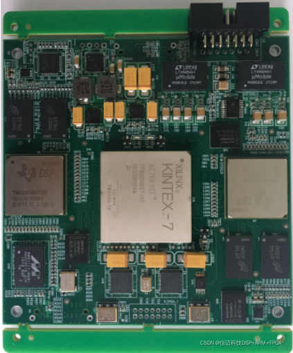
Figure 1: Development Board Physical Product
Shenzhen Xinmai's XM-C665xF-EVM, based on TI's design, is a DSP+FPGA high-speed big data acquisition and processing architecture, suitable for high-end image processing, high-speed big data transmission, and audio/video big data acquisition and processing fields. This design integrates the board cards through communication interfaces such as TMS320C665x's uPP, EMIF, I2C, PCIe, and SRIO, forming a DSP+FPGA architecture, thereby realizing a unique, flexible, and powerful DSP+FPGA high-speed data acquisition and processing system.
The SOM-XM665xF exposes all CPU resource signal pins, making secondary development extremely easy. Customers only need to focus on upper-layer applications, reducing development difficulty and time costs, enabling rapid product launch and timely market capture. It not only provides rich demo programs but also offers DSP inter-core communication development tutorials, comprehensive technical support, assisting customers with baseboard design and debugging, as well as multi-core software development.
2 Typical Application Areas
- Data acquisition, processing, and display systems for Telecom Towers: High-speed data acquisition and generation for Remote Radio Units (RRU)
- High-speed data acquisition and processing systems
- High-end image processing equipment
- High-end audio and video data processing
- Communication systems
3 Software and Hardware Parameters
- The front end uses an FPGA to acquire two channels of AD data, which is then transmitted to the DSP via communication interfaces such as uPP, EMIF bus, or PCIe, SRIO interfaces.
- After the AD data is processed by the DSP, it can be used for applications such as data comparison and analysis, network forwarding, and SATA hard disk storage.
- Based on the processing results, the DSP sends the resulting logic control commands to the FPGA, which then controls the on-board DA to achieve logic output at an update rate of 175MSPS.
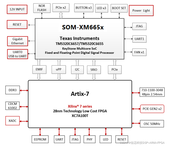
Figure 2: Big Data Acquisition Block Diagram
- The high-speed data acquisition front-end synchronously acquires two AD analog input signals via the FPGA, enabling pre-filtering of AD data, with a maximum AD sampling rate of 250MSPS. An additional DAC channel can output parallel DA data of arbitrary amplitude and waveform, with an update rate of 175MSPS.
- The high-speed data transmission section consists of communication interfaces such as EMIF, I2C, PCIe, and SRIO. Large-throughput AD and DA data can be transmitted at high speed and stably between the DSP and FPGA via SRIO and PCIe interfaces; the DSP can perform logic control and medium-throughput data exchange with the FPGA via the EMIF bus, and also perform initialization settings and parameter configuration on the FPGA side via I2C.
(3) The high-speed data processing section consists of the DSP core and algorithm libraries. It can perform real-time transformation processing of signal parameters such as time domain, frequency domain, and amplitude for AD and DA data (e.g., FFT transform, FIR filtering).
(4) The video acquisition and output expansion section consists of CameraLink input/output modules, VGA output modules, Gigabit Ethernet, and other components. With rich interface resources and flexible, convenient solution choices, it is an ideal choice for high-end image processing systems.
3.1 Hardware Parameters
Table 1 XM6678-EasyEVM Hardware Parameters
CPU
Single-core TMS320C6655 / Dual-core TMS320C6657, Main Frequency 1.0/1.25GHz
ROM
128/256MByte NAND FLASH
RAM
512M/1G Byte DDR3
EEPROM
1Mbit
FLASH
32/64Mbit SPI NOR FLASH
LED
1x Power indicator
1x Programmable indicator
Sensor
1x TMP102, Core board temperature sensor, I2C interface
Connectors
2x 50pin Male B2B, 2x 50pin Female B2B, Pitch 0.8mm, Mated Height 5.0mm, Total 200pin
1x 80pin High-speed B2B connector, Pitch 0.5mm, Mated Height 5.0mm, Signal rate up to 10GBaud
Expansion IO
2x 25pin IDC3 Simple Box Header, Pitch 2.54mm, including EMIF16 expansion signals
2x 25pin IDC3 Simple Box Header, Pitch 2.54mm, including SPI, I2C, TIMER, GPIO and other expansion signals
2x 25pin IDC3 Simple Box Header, Pitch 2.54mm, including TSIP expansion signals
1x SRIO 2.1 TX, 1x SRIO 2.1 RX, 4 channels, maximum communication rate 5GBaud per channel
1x PCIe 4x (Gen2), 2 channels, maximum communication rate 5GBaud per channel
1x HyperLink, maximum communication rate 40GBaud, ideal interface for KeyStone processor interconnection
Emulator Interface
1x 14pin TI Rev B JTAG interface, Pitch 2.54mm
Buttons
2x Reset buttons
1x Non-maskable interrupt button
1x User programmable button
Boot Mode
1x 5-bit boot mode, DIP switch selection
Network
2x Ethernet, 10/100/1000M adaptive
Serial Port
1x UART0, USB to serial port, provides 4-pin TTL level test port
1x UART1, DB9 interface, provides 6-pin TTL level test port
Fan Interface
1x FAN, 12V power supply, Pitch 2.54mm
Power Switch
1x Power DIP switch
Power Interface
1x 12V 3A DC input DC417 power interface, Outer diameter 4.4mm, Inner diameter 1.65mm
Note: Shenzhen Xinmai SOM-XM6655 and SOM-XM6657 core boards are pin-to-pin compatible in hardware.
Table 2 XM-A7HSAD Hardware Parameters
CPU
Xilinx Artix-7 XC7A100T FPGA
RAM
256Mbit NOR FLASH
ROM
2x 128M/256MByte DDR3
EEPROM
2KBit
Network
1x Ethernet, 10/100/1000M adaptive
LED
2x Power indicators
3x Programmable indicators
Buttons
2x Reset buttons
2x User programmable buttons
ADC
Dual channel, 1.8Vp-p, 12bit, max 250MHz sampling rate, LVDS signal output
DAC
175MHz, 12bit, max output current 5mA
XADC
Dual channel, 12bit, 1MHz, 1.25Vp-p
Expansion IO
1x SRIO TX, 1x SRIO RX, 4 channels, max single-channel rate 5GBaud, HDMI connector
1x PCIe 4x (Gen2), 2 channels, max single-channel communication rate 5GBaud
2x 48pin Euro-style connectors, GPIO expansion
1x I2C, HDMI connector
Emulator Interface
Boot Mode
1x 14pin JTAG interface, Pitch 2.00mm
1x 2-bit boot mode selection DIP switch
Serial Port
1x UART, Micro USB interface, provides 4-pin TTL level test port
Power Switch
1x Power DIP switch
Power Interface
1x 12V 2A DC input DC005 power interface, Outer diameter 5.5mm, Inner diameter 2.1mm
3.2 Software Parameters
Table 3
DSP Software Support
Bare-metal, SYS/BIOS operating system
CCS Version
CCS5.5
Software Development Kit Provided
MCSDK
Vivado Version
2015.2
4 Development Resources
(1) Provides core board pin definitions, editable baseboard schematics, editable baseboard PCBs, and chip datasheets, shortening hardware design cycles;
(2) Provides rich demo programs, including DSP multi-core communication tutorials, perfectly addressing multi-core development bottlenecks;
- Provides DSP and FPGA communication examples via PCIe, SRIO, I2C,