ZYNQ-Based WiFi Solution Implementation and Testing
The Sinming XM-ZYNQ7045-EVM is a software-defined radio (SDR) processing platform based on the Xilinx ZYNQ SoC. This platform uses a high-performance Xilinx ZYNQ series SoC, the XC7Z020, to enable transmission and reception of two channels of AD9361 wireless RF signals. It is widely used in applications such as SDR (software-defined radio), mobile base stations, WiFi, wireless LANs, and specialized or general-purpose wireless devices.
The ZYNQ7000 is Xilinx's latest generation extensible processing platform. The ZYNQ SoC integrates a dual-core ARM Cortex-A9 processor, seamlessly combining FPGA programmability with ARM's multimedia and video interfaces, making it ideal for low-power, cost-sensitive signal processing products.
High-speed HP interfaces enable data exchange between the PS (Processing System) and PL (Programmable Logic) domains. The PS side supports operating systems such as Linux and includes an embedded Gigabit Ethernet stack, simplifying TCP/IP-based Ethernet communication. The PL side contains abundant programmable logic resources for front-end signal processing.
1 Evaluation Board Overview
The Sinming XM-ZYNQ7045-EVM is a high-end heterogeneous multi-core SoC evaluation board based on the Xilinx Zynq-7000 series XC7Z045/XC7Z100 high-performance processors. The processor integrates a dual-core ARM Cortex-A9 in the PS domain and Kintex-7 architecture 28nm programmable logic resources in the PL domain. The evaluation board consists of a core board and a baseboard. The core board has undergone professional PCB layout and high/low temperature testing, ensuring stability and reliability suitable for various industrial applications.
The evaluation board provides rich interface resources, including dual Gigabit Ethernet ports, four SFP+ optical ports, CameraLink, HDMI, FMC HPC, GTX, PCIe, USB, and Micro SD interfaces, enabling users to rapidly evaluate product designs and conduct technology pre-research.
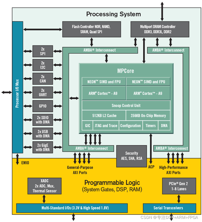
Figure 1 Xilinx Zynq-7000 Processor Functional Block Diagram
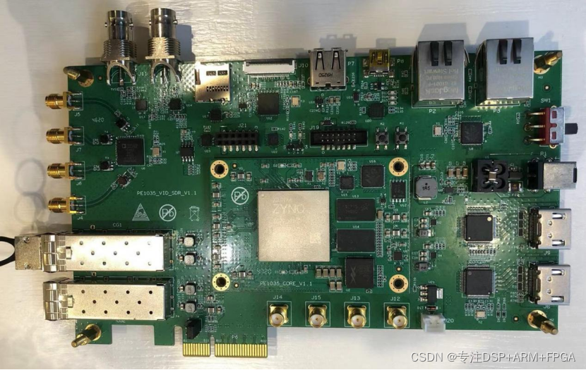
Figure 2
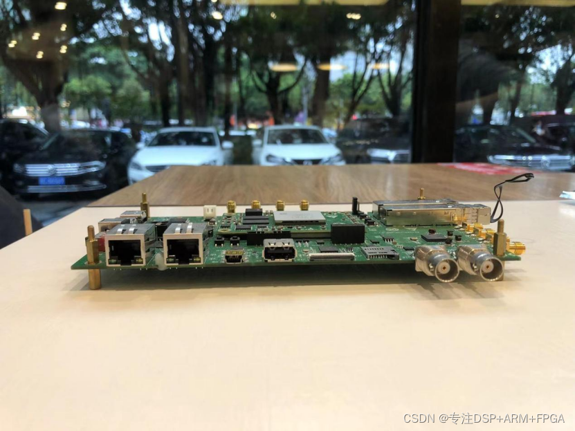
Figure 3
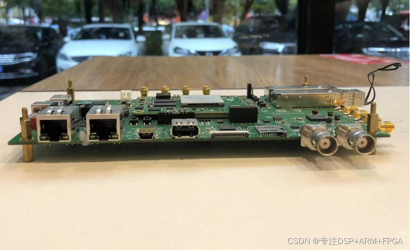
Figure 4
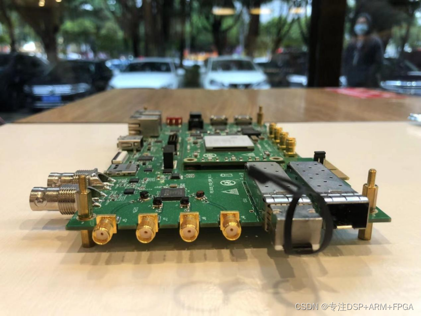
Figure 5
2 Typical Application Areas
- Software-defined radio
- Radar detection
- Optoelectronic detection
- Video tracking
- Image processing
- Underwater detection
- Positioning and navigation
- Deep learning
3 Hardware and Software Specifications
3.1 Hardware Specifications
Table 1
CPU
CPU: Xilinx Zynq-7000 XC7Z045/XC7Z100-2FFG900I
2x ARM Cortex-A9, 800MHz main frequency, 2.5DMIPS/MHz per core
1x Kintex-7 architecture programmable logic resources
ROM
PS side: 8GB eMMC
PS side: 128/256Mbit SPI NOR FLASH
RAM
PS: Single-channel 32-bit DDR bus, 1GB DDR3
PL: Single-channel 32-bit DDR bus, 1/2GB DDR3
Logic Cell
XC7Z045: 350K, XC7Z100: 444K
OSC
PS side: 33.33MHz
B2B Connector
2x 140-pin male high-speed B2B connectors, 2x 140-pin female high-speed B2B connectors, total 560 pins
Pitch: 0.5mm, mating height: 7.0mm
LED
2x power indicator LEDs (1 on core board, 1 on baseboard)
1x PL DONE LED (on core board)
3x PS user-programmable LEDs (2 on core board, 1 on baseboard)
2x PL user-programmable LEDs (2 on baseboard)
KEY
1x power reset button
1x system reset button
1x PS user input button
1x PL user input button
SD
1x Micro SD interface (PS side)
XADC
1x pin header interface, 2x 2-pin, 2.54mm pitch, single-channel dedicated differential input, 1MSPS
Ethernet
1x PS RGMII, RJ45 interface, 10/100/1000M auto-negotiation (PHY located on core board)
1x PL RGMII, RJ45 interface, 10/100/1000M auto-negotiation
Watchdog
1x Watchdog, 3-pin header, 2.54mm pitch, configurable via jumper cap
UART
1x Debug UART, Micro USB interface (PS side)
1x RS232 UART, DB9 interface (PL side)
1x RS485 UART, 3-pin 3.81mm green terminal block (PL side)
CAN
2x CAN, 3-pin 3.81mm green terminal block (PL side)
USB
4x USB 2.0 HOST interfaces, expanded via HUB (PHY located on core board)
PCIe
1x PCIe, derived from two GTX lanes, two lanes total, x4 edge connector (PL side)
IO
1x 400-pin FMC connector, 1.27mm pitch, HPC standard
SATA
1x 7-pin SATA interface, 150MHz LVDS differential clock (PL side)
HDMI
1x HDMI OUT (PL side)
1x HDMI IN (PL side)
DISPLAY
1x LCD RES resistive touch screen, 40-pin FFC connector, 0.5mm pitch (PL side)
CAMERA
2x CAMERA, 2x 10-pin female headers, 2.54mm pitch (PL side)
CameraLink
2x CameraLink Base interfaces, supporting Full mode (PL side)
SFP+
4x SFP+ optical ports, supporting 10G optical modules, driven by high-speed serial transceivers (GTX)
LVDS
1x pin header interface, 2x 15-pin, compatible with general-purpose LVDS displays, 2.00mm pitch (PL side)
SMA
1x GTX CLK
1x GTX RX
1x GTX TX
RTC
1x RTC socket, compatible with ML2032 (3V rechargeable) or CR2032 (3V non-rechargeable) coin cell batteries
FAN
1x FAN, 3-pin header terminal block, 12V power supply, 2.54mm pitch
JTAG
1x 14-pin JTAG interface, 2.0mm pitch
BOOT SET
1x 6-bit DIP switch for boot mode selection
SWITCH
1x power toggle switch
POWER
1x 12V/6A DC input DC-005 power jack, compatible with 5.5mm outer diameter, 2.1mm inner diameter plug
3.2 Software Specifications
Table 2
ARM-side Software Support
Bare metal, FreeRTOS, Linux-4.9.0
Vivado Version
2017.4
Software Development Kits Provided
PetaLinux-2017.4, Xilinx SDK 2017.4, Xilinx HLS 2017.4
Driver Support
SPI NOR FLASH
DDR3
USB 2.0
eMMC
LED
KEY
RS485
MMC/SD
Ethernet
CAN
7-inch Touch Screen LCD (Resistive)
XADC
I2C
USB 4G
USB WiFi
RS232
4 Development Resources
(1) Provide core board pin definitions, editable baseboard schematics, editable baseboard PCB, and chip datasheets to shorten hardware design cycles;
(2) Provide system image files, kernel driver source code, file system source code, and a rich set of demo programs;
(3) Provide a complete platform development package and getting-started tutorials to save software integration time and simplify application development;
(4) Provide detailed PS + PL SoC architecture communication tutorials to effectively overcome heterogeneous multi-core development bottlenecks.
Main development examples include: Ø
- Linux-based development examples
- Bare-metal development examples
- FreeRTOS-based development examples
- PS + PL heterogeneous multi-core development examples
- OpenAMP-based Linux + bare-metal/FreeRTOS dual-core ARM communication examples
- HDL and HLS development examples based on PL
- Qt development examples
- CameraLink, SDI, HDMI, PAL video input/output examples
- High-speed AD (AD9613) acquisition + high-speed DA (AD9706) output examples
- AD9361 software-defined radio examples
- UDP (10G) optical interface communication examples
- Aurora optical interface communication examples
- PCIe communication examples
5 Electrical Characteristics
Operating Environment
Parameter
Minimum
Typical
Maximum
Core Board Operating Temperature
-40°C
/
85°C
Core Board Operating Voltage
/
5.0V
/
Baseboard Operating Voltage
/
12.0V
/
Power Consumption Test
Category
Operating State
Typical Voltage
Typical Current
Typical Power
Core Board
State 1
5.0V
0.40A
2.00W
State 2
5.0V
1.85A
9.25W
Baseboard
State 1
12.0V
0.43A
5.16W
State 2
12.0V
1.19A
14.28W
Note: Power consumption measured using core board with XC7Z045 CPU. Power consumption varies depending on application scenario; data is for reference only.
State 1: Evaluation board without external modules, PS system booted without running additional applications; PL running LED test program.
State 2: Evaluation board without external modules, PS system booted, running DDR stress read/write test program with approximately 100% utilization on both ARM Cortex-A9 cores; PL running IFD comprehensive test program.
Figure 11 Resource Utilization in State 2
6 Mechanical Dimensions
Table 4
Core Board
Baseboard
PCB Dimensions
62mm × 100mm
142.75mm × 260mm
PCB Layers
14 layers
8 layers
PCB Thickness
1.6mm
1.6mm
Number of Mounting Holes
4
4
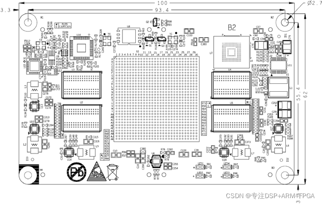
Figure 12 Core Board Mechanical Dimensions
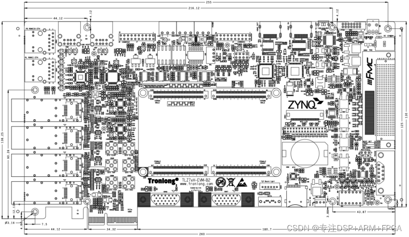
Figure 13 Baseboard Mechanical Dimensions
7 Technical Support
- Assist in baseboard design and testing to reduce hardware design errors;
- Assist in resolving anomalies encountered during operation per user manual;
- Assist in product fault diagnosis;
- Assist in correctly compiling and running provided source code;
- Assist in secondary product development;
- Provide long-term after-sales support.
8 Value-Added Services
- Custom motherboard design
- Custom core board design
- Embedded software development
- Joint project development
- Technical training
For more information, please contact Sinming Technology, Shenzhen.