ZYNQ-based Data Storage and Real-time Imaging System
This article introduces a data storage and real-time imaging system, primarily addressing the issues of complex structure, long development cycles, and lack of portability in existing imaging systems.
1 Evaluation Board Introduction
Xinmai Technology XM-ZYNQ7045-EVM is a high-end heterogeneous multi-core SoC evaluation board designed based on Xilinx Zynq-7000 series XC7Z045/XC7Z100 high-performance processors. The processor integrates a PS-side dual-core ARM Cortex-A9 + PL-side Kintex-7 architecture 28nm programmable logic resources. The evaluation board consists of a core board and an evaluation baseboard. The core board has undergone professional PCB layout and high/low temperature testing, ensuring stability and reliability, and meeting the requirements of various industrial application environments.
The evaluation board offers rich interface resources, providing dual Gigabit Ethernet ports, four SFP+ optical ports, CameraLink, HDMI, FMC HPC, GTX, PCIe, USB, Micro SD, and other interfaces, facilitating users in quickly evaluating product solutions and conducting technical preliminary research.
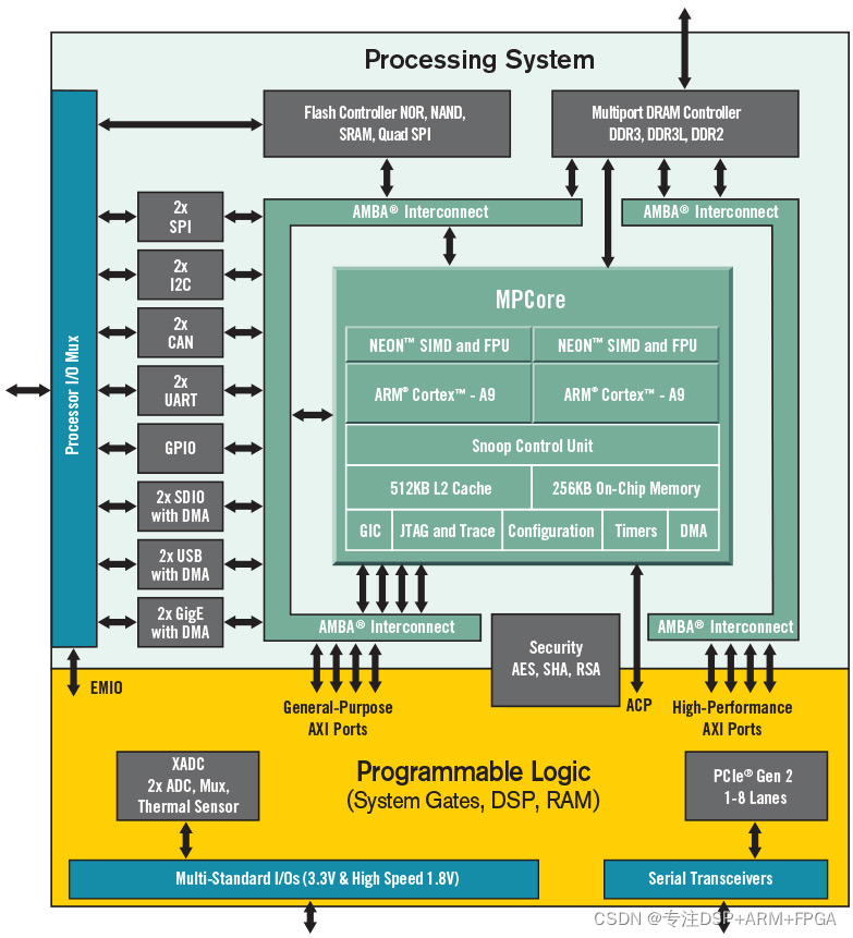
Figure 1 Xilinx Zynq-7000 Processor Functional Block Diagram
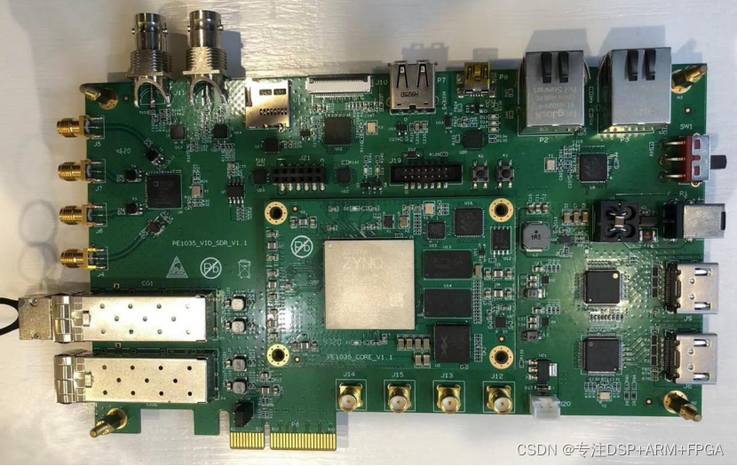
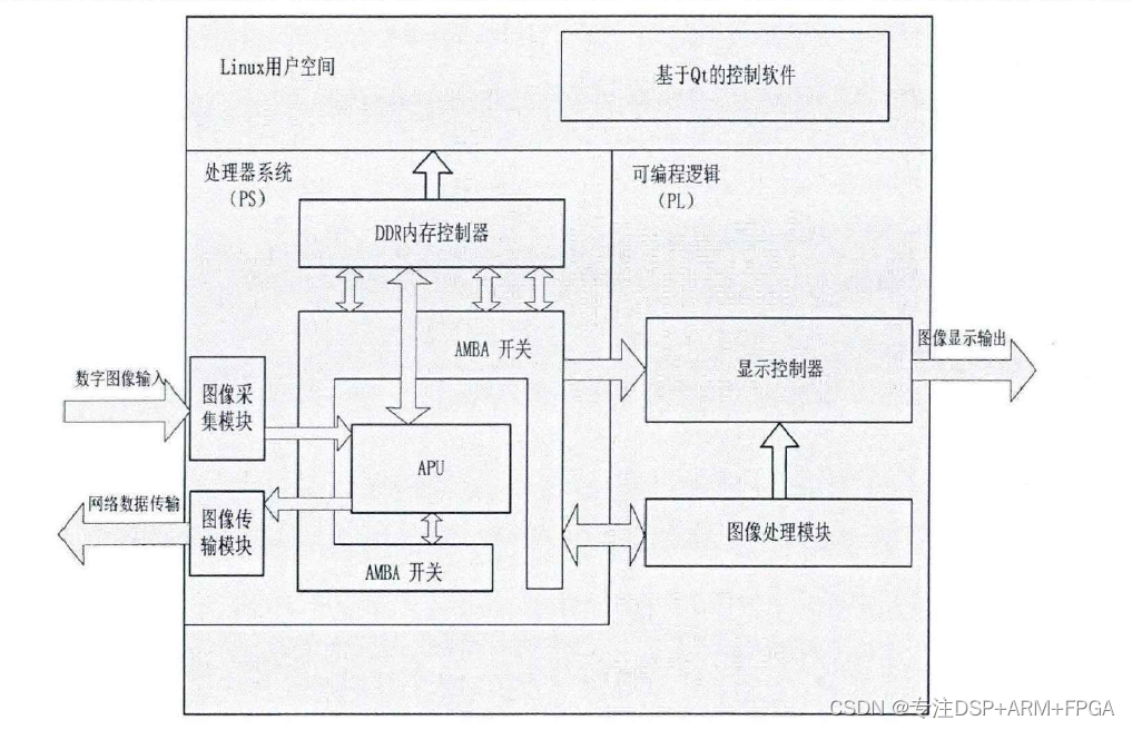
Figure 2
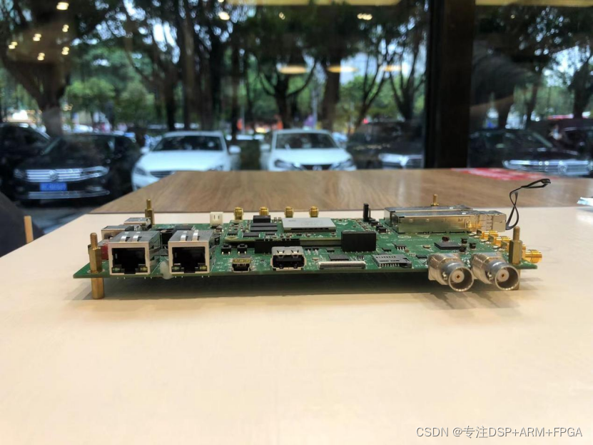
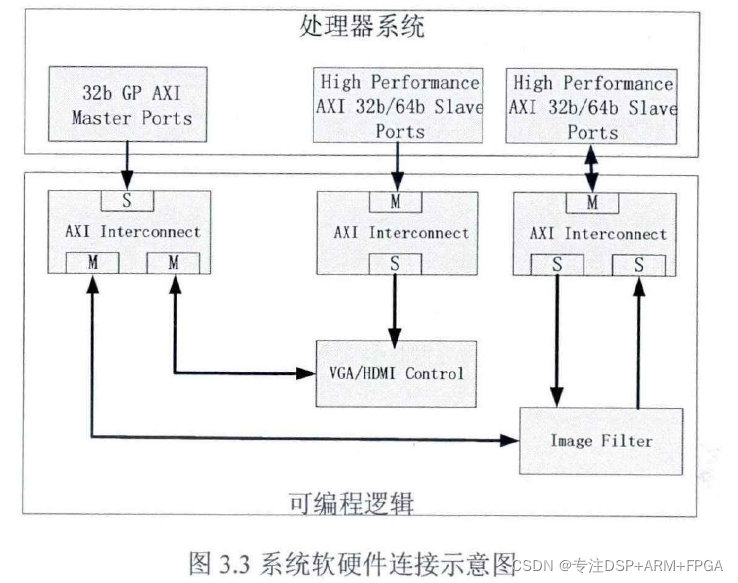
Figure 3
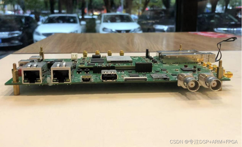
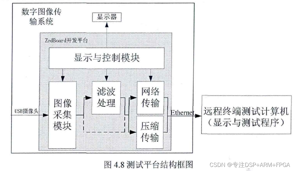
Figure 4
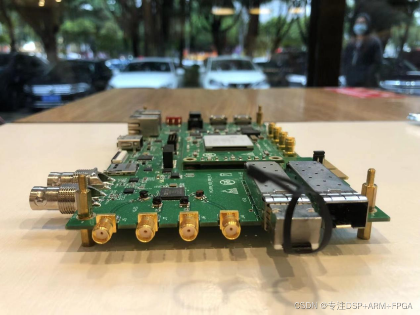
Figure 5
2 Typical Application Areas
- Software Defined Radio
- Radar Detection
- Optoelectronic Detection
- Video Tracking
- Image Processing
- Underwater Detection
- Positioning and Navigation
- Deep Learning
3 Software and Hardware Parameters
3.1 Hardware Parameters
Table 1
CPU
Xilinx Zynq-7000 XC7Z045/XC7Z100-2FFG900I
2x ARM Cortex-A9, main frequency 800MHz, 2.5DMIPS/MHz Per Core
1x Kintex-7 architecture programmable logic resources
ROM
PS side: 8GByte eMMC
PS side: 128/256Mbit SPI NOR FLASH
RAM
PS: Single-channel 32bit DDR bus, 1GByte DDR3
PL: Single-channel 32bit DDR bus, 1/2GByte DDR3
Logic Cell
XC7Z045: 350K, XC7Z100: 444K
OSC
PS side: 33.33MHz
B2B Connector
2x 140pin male high-speed B2B connectors, 2x 140pin female high-speed B2B connectors, total 560pin, pitch 0.5mm, mated height 7.0mm
LED
2x Power indicator LEDs (1 on core board, 1 on evaluation baseboard)
1x PL side DONE LED (1 on core board)
3x PS side user-programmable LEDs (2 on core board, 1 on evaluation baseboard)
2x PL side user-programmable LEDs (2 on evaluation baseboard)
KEY
1x Power reset button
1x System reset button
1x PS side user input button
1x PL side user input button
SD
1x Micro SD interface (PS side)
XADC
1x Pin header interface, 2x 2pin specification, 2.54mm pitch, single-channel dedicated differential input, 1MSPS
Ethernet
1x PS RGMII, RJ45 interface, 10/100/1000M adaptive (PHY located on core board)
1x PL RGMII, RJ45 interface, 10/100/1000M adaptive
Watchdog
1x Watchdog, 3pin pin header, 2.54mm pitch, configured via jumper cap
UART
1x Debug UART, Micro USB interface (PS side)
1x RS232 UART, DB9 interface (PL side)
1x RS485 UART, 3pin 3.81mm green terminal block (PL side)
CAN
2x CAN, 3pin 3.81mm green terminal block (PL side)
USB
4x USB 2.0 HOST interfaces, expanded using HUB (PHY located on core board)
PCIe
1x PCIe, derived from two GTX groups, total two channels, x4 gold finger connection (PL side)
IO
1x 400pin FMC connector, 1.27mm pitch, HPC standard
SATA
1x 7pin SATA interface, 150MHz LVDS differential clock (PL side)
HDMI
1x HDMI OUT (PL side)
1x HDMI IN (PL side)
DISPLAY
1x LCD RES resistive touchscreen, 40pin FFC connector, 0.5mm pitch (PL side)
CAMERA
2x CAMERA, 2x 10pin female header, 2.54mm pitch (PL side)
CameraLink
2x CameraLink Base interfaces, supporting Full mode (PL side)
SFP+
4x SFP+ optical ports, supporting 10 Gigabit optical modules, derived from high-speed serial transceivers (GTX)
LVDS
1x Pin header interface, 2x 15pin specification, connectable to general-purpose LVDS displays, 2.00mm pitch (PL side)
SMA
1x GTX CLK
1x GTX RX
1x GTX TX
RTC
1x RTC socket, compatible with button cells ML2032 (3V rechargeable), CR2032 (3V non-rechargeable)
FAN
1x FAN, 3pin pin header terminal, 12V power supply, 2.54mm pitch
JTAG
1x 14pin JTAG interface, 2.0mm pitch
BOOT SET
1x 6bit boot mode selection DIP switch
SWITCH
1x Power toggle switch
POWER
1x 12V6A DC input DC-005 power interface, connectable to power plugs with outer diameter 5.5mm, inner diameter 2.1mm
3.2 Software Parameters
Table 2
ARM side software support
Bare metal, FreeRTOS, Linux-4.9.0
Vivado version
2017.4
Software development kit provided
PetaLinux-2017.4, Xilinx SDK 2017.4, Xilinx HLS 2017.4
Driver support
SPI NOR FLASH
DDR3
USB 2.0
eMMC
LED
KEY
RS485
MMC/SD
Ethernet
CAN
7in Touch Screen LCD(Res)
XADC
I2C
USB 4G
USB WIFI
RS232
4 Development Resources
(1) Provides core board pin definitions, editable baseboard schematics, editable baseboard PCBs, and chip datasheets, shortening hardware design cycles;
(2) Provides system firmware images, kernel driver source code, file system source code, and rich demo programs;
(3) Provides complete platform development kits and getting started tutorials, saving software organization time and making application development simpler;
(4) Provides detailed PS + PL SoC architecture communication tutorials, perfectly addressing heterogeneous multi-core development bottlenecks.
Development examples mainly include: Ø
- Linux-based development routines
- Bare-metal-based development examples
- FreeRTOS-based development examples
- PS + PL-based heterogeneous multi-core development examples
- OpenAMP-based Linux + Bare-metal/FreeRTOS dual-core ARM communication development examples
- PL-side HDL, HLS development examples
- Qt development examples
- CameraLink, SDI, HDMI, PAL video input/output examples
- High-speed AD (AD9613) acquisition + high-speed DA (AD9706) output examples
- AD9361 Software Defined Radio examples
- UDP (10G) optical port communication examples
- Aurora optical port communication examples
- PCIe communication examples