XM6748F-IDK TMS320C6748+FPGA High-Speed Data Acquisition and Processing Platform
Supports 32-channel AD acquisition and 32-channel DA output.
Supports multiple RS485 and RS232 serial ports;
Supports real-time systems and control latency;
Supports multi-core communication between DSP and ARM, providing rich sampling demos;
Supports graphical interface programming, with touch control!
- C6748+FPGA Development Board Introduction The XM6748F-IDK-V3, designed by Shenzhen Xinmai, is a DSP+FPGA high-speed data acquisition and processing development board, suitable for data acquisition and processing applications in power, communication, industrial control, medical, and audio/video fields.
This design adopts the OMAP-L138+Spartan-6 platform, where OMAP-L138 is Texas Instruments' (TI) low-power, high-performance floating-point DSP C6748+ARM9 dual-core processor, and Spartan-6 is Xilinx's highly cost-effective FPGA processor with flexible platform upgrade capabilities. This design integrates the two chips via communication interfaces such as OMAP-L138's uPP and EMIF. The internal DSP and ARM of the OMAP-L138 communicate through DSPLINK/SYSLINK for dual-core communication, realizing a unique, flexible, and powerful DSP+ARM+FPGA tri-core high-speed data acquisition and processing system.
- OMAP-L138+FPGA Development Board Resource Block Diagram
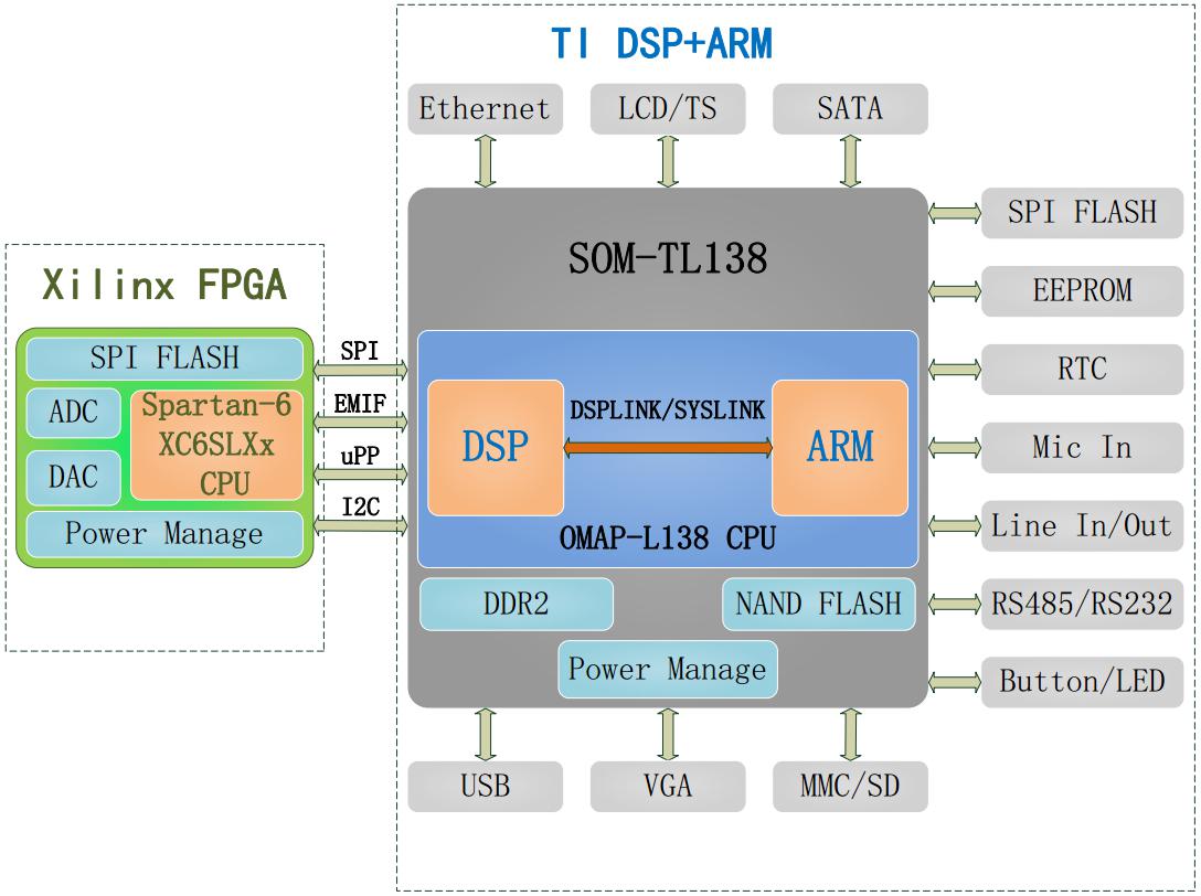
Figure 1 OMAP-L138+FPGA Tri-Core High-Speed Data Acquisition and Processing Resource Block Diagram
Framework Analysis:
The front end, consisting of a Xilinx Spartan-6 XC6SLX9/16/25/45 FPGA, acquires two channels of AD data, with a maximum sampling rate of 65MHz. The AD data is transmitted to the OMAP-L138's DSP via the uPP or EMIF bus. After the data is processed by the DSP, it is sent to the ARM via DSPLINK or SYSLINK dual-core communication components for applications such as application interface development, network forwarding, and SATA hard drive storage. Based on the processing results, the OMAP-L138's DSP or ARM sends the resulting logical control commands to the FPGA. The FPGA then controls the on-board DA to realize logical output, with an update rate of 175 MSPS. (1) The high-speed data acquisition front-end section, consisting of a Xilinx Spartan-6 XC6SLX9/16/25/45 FPGA, simultaneously acquires two channels of AD analog input signals. It can perform pre-filtering on AD data, with a maximum AD sampling rate of 65 MSPS. Another DAC channel can output parallel DA data of arbitrary amplitude and waveform, with an update rate of 175 MSPS.
(2) The high-speed data transmission section consists of uPP, EMIF, SPI, and I2C communication buses. Large-throughput AD and DA data can be transmitted at high speed and stably between the DSP and FPGA via the uPP bus; the DSP can perform parallel logic control and medium-throughput data exchange with the FPGA via the EMIF bus; the ARM can perform initial setup and parameter configuration for the FPGA via SPI and I2C.
(3) The high-speed data processing section consists of the DSP core and algorithm libraries. It can perform real-time transformation processing of signal parameters such as time domain, frequency domain, and amplitude for AD and DA data (e.g., FFT transform, FIR filtering).
(4) The DSP+ARM dual-core communication section consists of the DSP core, ARM core, and DSPLINK/SYSLINK dual-core communication components. Data exchange and communication between the DSP and ARM dual cores are achieved through memory sharing.
(5) The data display, storage, and expansion section consists of the ARM core, graphical display, network, and SATA hard drive components. The ARM application interface can display real-time time-domain and frequency-domain waveforms of AD and DA data; it also enables big data storage and remote network communication.
- Xilinx Spartan-6 FPGA High-Speed Data Acquisition Front-End Logic Implementation
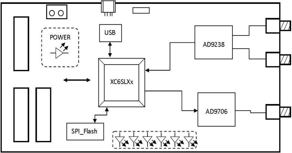
Xilinx Spartan-6 FPGA – XC6SLXx
The XC6SLXx is a widely used and highly cost-effective FPGA platform in the Xilinx Spartan-6 series. It has 324 pins, provides a large number of available I/Os, offers excellent platform upgrade capabilities, reasonable hardware cost differences, and smooth scalability. Models such as LX9, LX16, LX25, and LX45 can be used according to actual needs. Furthermore, the four CPU models are pin-to-pin compatible.
(1) XC6SLX9: Interface level, with interface programming and clock control capabilities.
(2) XC6SLX16: Algorithm level, capable of simple algorithm processing.
(3) XC6SLX25: Algorithm level, capable of intermediate algorithm processing.
(4) XC6SLX45: System level, capable of meeting more complex algorithm and system logic processing requirements.
High-Speed ADC – AD9238
The AD9238 is a 12-bit dual-channel A/D converter launched by ADI, featuring the industry's fastest sampling rate. It offers selectable voltage input ranges of 1Vp-p and 2Vp-p, and is widely used in high-speed data acquisition applications such as power, communication, industrial control, and medical.
The AD9238 comes in three models with sampling rates of 20 MS/s, 40 MS/s, and 65 MS/s, respectively. It not only provides excellent dynamic performance comparable to single-channel A/D converters but also offers better anti-crosstalk performance compared to using two single-channel A/D converters. The three models are pin-to-pin compatible and can be flexibly configured according to actual needs.
The three AD9238 models have power consumptions of 180mW, 330mW, and 600mW, respectively, which is only half the power consumption of comparable A/D converters. They adopt a 64-pin LQFP package (size only 9mm x 9mm), making them ideal for applications with strict size requirements.
High-Speed DAC – AD9706
The AD9706 is a 12-bit D/A converter launched by ADI, with an update rate of 175 MSPS