OMAPL138 + FPGA AD7606 Data Acquisition Test
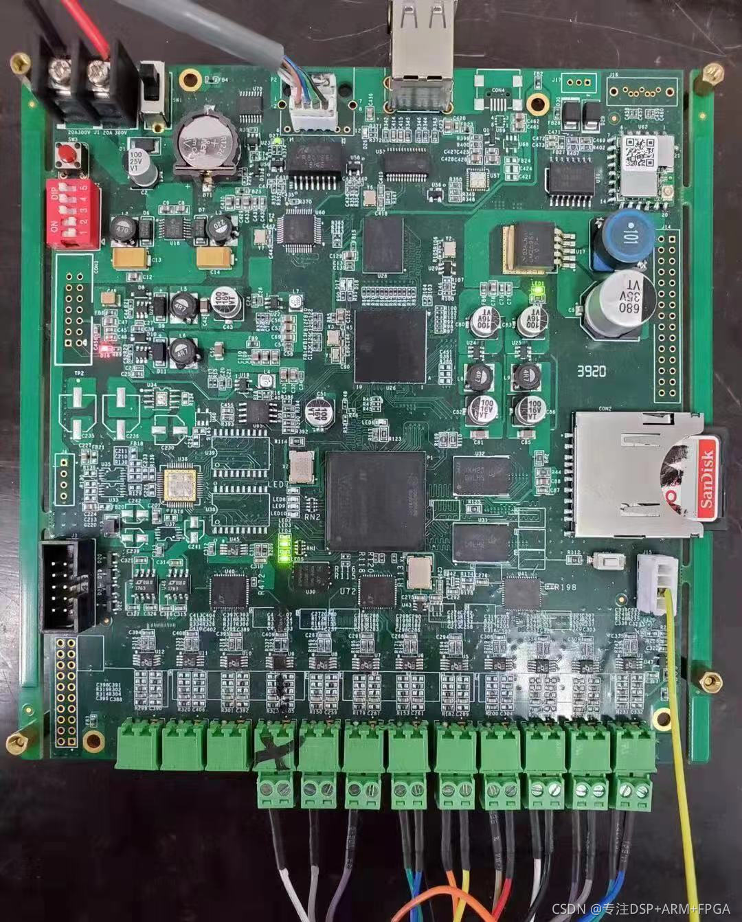
The development board used for this test is the Ximai OMAPL138+FPGA multi-core heterogeneous development board XM138F-IDK-V3.
This program implements reading and writing to the AD7606 ADC chip using the EMIFA bus. The AD7606 is an 8-channel, 16-bit ADC chip with a 200K sampling rate. It supports parallel port/serial port read/write modes. The module defaults to parallel port mode, which allows a sampling rate of up to 200K. In SPI mode, the sampling rate is only about 100K. It is strongly recommended to use parallel port mode to fully utilize the synchronous sampling performance of the 8-channel AD7606. It supports bipolar signal input of ±10V or ±5V and is widely used in industries such as power and instrumentation. For more information, please refer to the Ximai AD7606 Data Acquisition Module XM7606 datasheet.
The input voltage range can be set to ±10V or ±5V by configuring the jumper on J1 of the AD7606 data acquisition module XM7606. Connecting to '0' sets the range to ±5V, and connecting to '1' sets the range to ±10V. The circuit diagram is shown below:
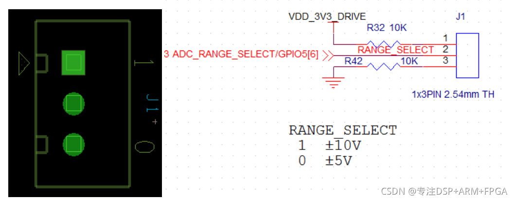
Figure 289 J1 Connector Pin Definition
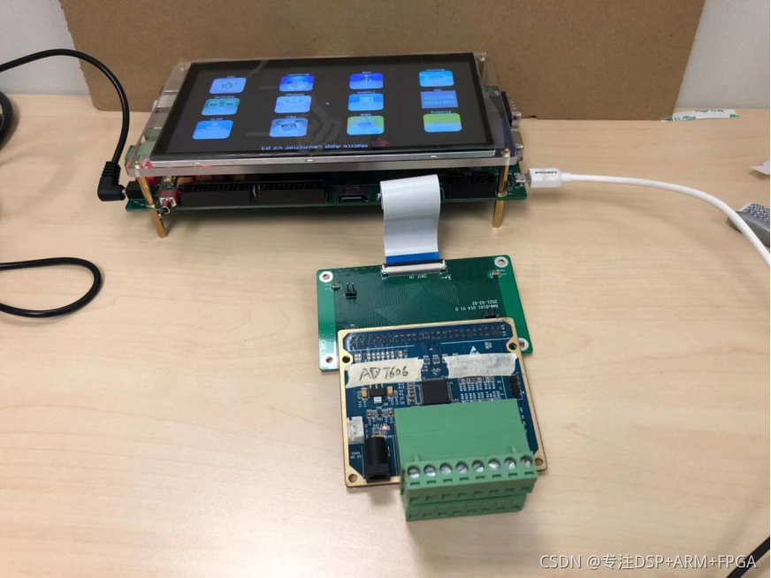
- Connect the Development Board
Taking the Ximai XM138F-IDK-V3 development board as an example, insert the XM7606 module into the J2 interface of the development board's baseboard, as shown in the figure below. Do not connect it to the J3 interface on the baseboard, as this may damage the module. Also, check for any left/right misalignment.
- Connect Voltage Signals and Power Supply
Connect the voltage signals to be acquired to the corresponding channels, and the other end to the corresponding ground, for example, connect to V1 and V1GND. Upper layer signals: V1, V2, V3, V4, V5, V6, V7, V8 (from left to right in order); Lower layer signals: V1GND, V2GND, V3GND, V4GND, V5GND, V6GND, V7GND, V8GND (from left to right in order). Also, power the module using a 5V2A power adapter.
Note: The input voltage must not exceed the set voltage range, otherwise the module may be damaged. For testing convenience, only one channel's ground was connected here; the grounds of all 8 channels are internally connected. The input terminals of all 8 channels were also simultaneously connected to the same digital input power supply.
- Start the Development Board
Load the EMIF_AD7606.out file according to the project import steps, then click the program run button.
- Read ADC Sample Values
The serial debug terminal will print information similar to the following, as shown in the figure below:
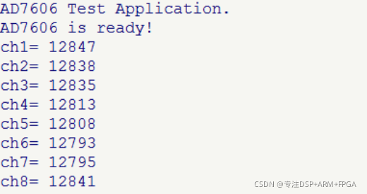
Figure 292
Theoretical Value Calculation Method
For example, when inputting 2.0V, the theoretical value obtained is:
**Value=**32768*2.0/5.0=13107
For the source code and reference design circuits for C6748 and FPGA communication via EMIFA, please refer to the CD-ROM materials for the FPGA high-speed data acquisition board card accompanying the C6748.
Supports 32-channel ADC acquisition and 32-channel DAC output. Supports multiple RS485 and RS232 serial ports; Supports real-time systems and control latency; Supports multi-core communication between DSP and ARM, providing rich sampling demos; Supports graphical interface programming and touch control!