Design and Implementation of a 48-Channel Data Acquisition System Based on OMAPL138 + FPGA
In the current global situation, with the world's population continuing to grow and pressure on land resources and the environment increasing, the ocean has objectively become a global reserve resource base and a successor area for certain key strategic resources. To further explore the ocean, humanity has introduced digital signal and image processing technologies into the hydroacoustic field, leading to the creation of various new types of sonar arrays.
This paper designs a data acquisition system based on the recording requirements for electro-acoustic signals converted from a 48-element sonar array. The content includes the overall scheme design, hardware circuit design, and software program design of the acquisition system. The data acquisition system uses an FPGA and an OMAP-L138 processor as its control core. After the core controller design was completed, six multi-channel high-precision analog-to-digital converter (ADC) chips were used to synchronously acquire electro-acoustic conversion signals from 48 channels. To ensure multiple systems work collaboratively underwater, a synchronizer module was designed to manage timing, ensuring all systems begin data acquisition at precise, absolute time points. A large-capacity SATA hard drive is used to store the acquired data, named according to the time information provided by the synchronizer module. This facilitates subsequent data processing and supports the real-time performance and reliability verification of field data. In the laboratory, the intended functions of the acquisition system were verified, and its system performance was tested from various aspects. Actual testing confirmed that the functional and real-time performance indicators of the data acquisition system designed in this paper meet expectations. The collected and stored data is accurate and valid, indicating the acquisition system is ready for deployment. Finally, to further ascertain the stability of the acquisition system, the project team conducted field experiments in a pool and in the waters off Sanya. The successful completion of these experiments demonstrated the stable operation of the acquisition system.
1 Evaluation Board Introduction
- Based on TI OMAP-L138 (fixed/floating-point DSP C674x + ARM9) + Xilinx Spartan-6 FPGA processor;
- OMAP-L138 and FPGA are connected via uPP, EMIFA, and I2C buses, with communication speeds up to 228 MByte/s; OMAP-L138 has a main frequency of 456MHz, offering computing power up to 3648 MIPS and 2746 MFLOPS;
- FPGA compatible with Xilinx Spartan-6 XC6SLX9/16/25/45, offering strong platform upgrade capabilities;
- The development board provides rich peripheral interfaces, including high-speed data transfer interfaces such as Gigabit Ethernet, SATA, EMIFA, uPP, USB 2.0, as well as common interfaces like GPIO, I2C, RS232, PWM, and McBSP;
- Certified through high and low-temperature testing, suitable for various harsh working environments;
- DSP+ARM+FPGA triple-core SOM (System-on-Module), with dimensions of 66mm*38.6mm, using industrial-grade B2B connectors to ensure signal integrity; Ø
- Supports bare-metal, SYS/BIOS operating system, and Linux operating system.
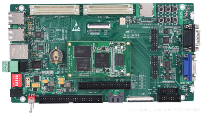 Figure 1 Front and Side View of the Development Board
The XM138F-IDK-V3.0 is a development board designed by Shenzhen Xinmai based on the XM138-SP6-SOM core board. It features a 4-layer board design with immersion gold and lead-free processes, providing users with a test platform for the XM138-SP6-SOM core board to quickly evaluate its overall performance.
The XM138-SP6-SOM exposes all CPU resource signal pins, making secondary development extremely easy. Customers only need to focus on upper-layer applications, significantly reducing development difficulty and time costs, enabling rapid product launch and timely capture of market opportunities. It not only provides rich demo programs but also detailed development tutorials and comprehensive technical support to assist customers with baseboard design, debugging, and software development.
2 Typical Application Areas
- Data Acquisition, Processing, and Display Systems
- Smart Power Systems
- Image Processing Equipment
- High-Precision Instrumentation
- Mid-to-High-End CNC Systems
- Communication Equipment
- Audio and Video Data Processing
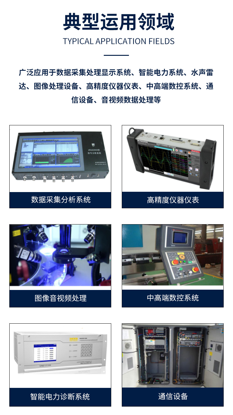 Figure 2 Typical Application Areas
3 Hardware and Software Parameters
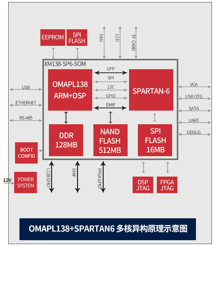 Schematic Diagram of Development Board Peripheral Resources Block Diagram
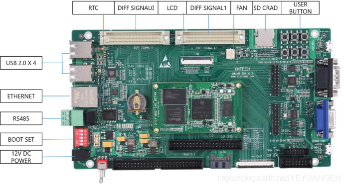
Figure 3 Schematic Diagram of Development Board Interfaces
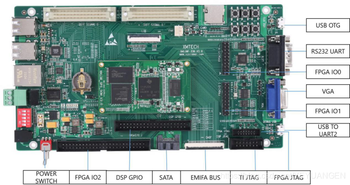
Figure 4 Schematic Diagram of Development Board Interfaces