OMAPL138+FPGA-based IF Data Acquisition and Storage System for Ship Automatic Identification System
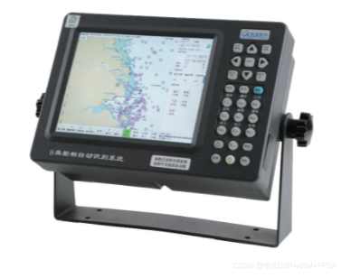
The Automatic Identification System (AIS) is a digital navigation aid used at sea for collision avoidance and vessel identification, playing a significant role in maintaining maritime traffic safety. The position information for the AIS system is provided by the Global Navigation Satellite System (GNSS). To enhance the reliability of the AIS system, alternative positioning systems for GNSS, specifically land-based positioning systems, are currently being researched in the maritime domain. A ship autonomous positioning system based on AIS shore stations has been developed. During the research process of this system, to analyze and process real-time signal information from AIS and GNSS, it is necessary to acquire and store the intermediate frequency (IF) data of both AIS and GNSS. This facilitates the detection and evaluation of these signals and provides a large volume of raw data for future use, holding significant value in terms of practical application and research.
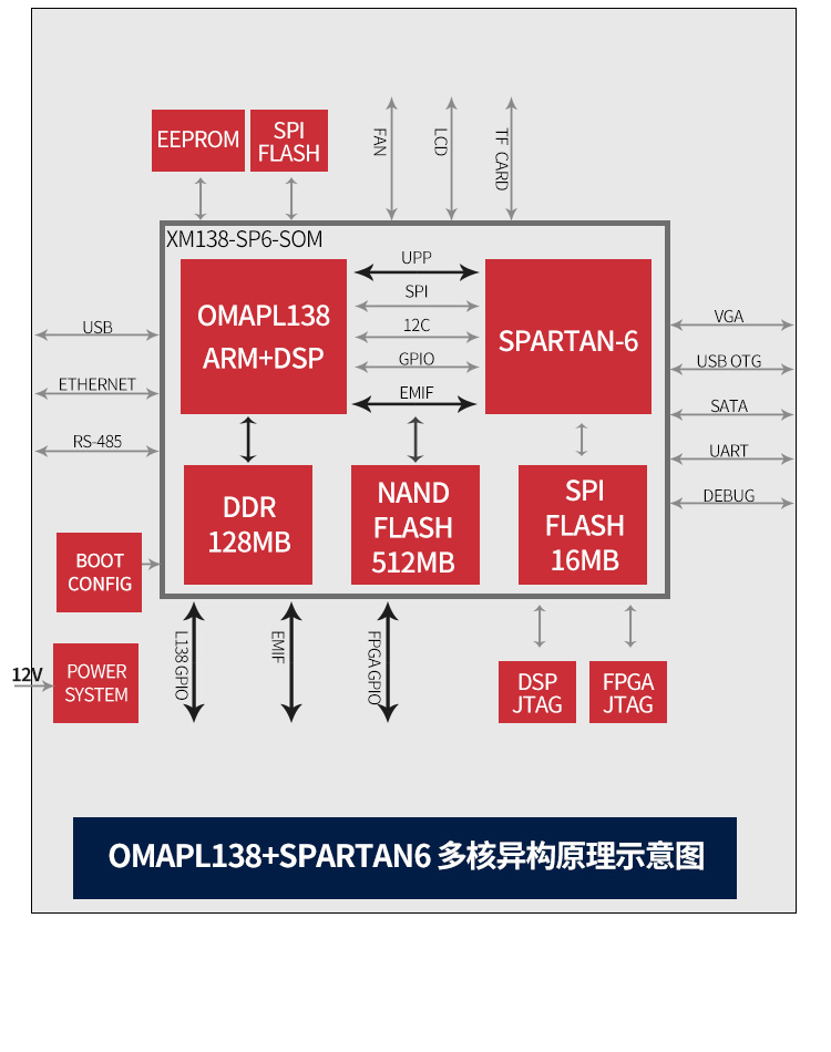
This paper designs an IF data acquisition and storage system based on an embedded triple-core platform, capable of acquiring and storing IF data. The designed hardware platform includes an acquisition module, a Xilinx Spartan-6 + OMAPL138 triple-core platform, and a SATA storage device. Specifically, an ADS830E acquisition chip performs the acquisition of AIS signals, and the data is transmitted to the triple-core platform's FPGA I/O port via an interface adapter module. An NJ1006A RF front-end receives signals from the GPS antenna, passes them through a level shifting module, and is powered by a power supply module along with the level shifting module. The output of the level shifting module is connected to the triple-core platform's FPGA I/O port, and finally, the data is stored on a SATA hard drive. The system software is divided into three parts: acquisition, transmission, and storage. The acquisition program controls the timing and data reception of the acquisition chip, written in Verilog, and runs on the FPGA. The transmission program includes DSP's DMA reception of uPP data and data access by the two processors in shared memory. The DSP and ARM run SYS/BIOS and Linux operating systems, respectively, and data interaction is achieved using TI's SYSLINK dual-core communication component. The finally acquired data is stored on the SATA hard drive. After data storage is complete, system platform testing and verification are performed. The acquired and stored AIS IF digital data is reconstructed into waveforms in Matlab, and a Fast Fourier Transform (FFT) is performed. The results are compared with the signal source waveforms and center frequencies measured on an oscilloscope to verify their accuracy. At the FPGA's GPS IF data reception end, the CHIPSCOPE tool is used to check if the waveform matches the program logic, thereby verifying its accuracy.
1 Evaluation Board Introduction
- Based on TI OMAP-L138 (fixed-point/floating-point DSP C674x + ARM9) + Xilinx Spartan-6 FPGA processor;
- OMAP-L138 FPGA is connected via uPP, EMIFA, and I2C buses, with communication speeds up to 228 MByte/s; OMAP-L138 main frequency is 456MHz, with computing power up to 3648 MIPS and 2746 MFLOPS;
- FPGA is compatible with Xilinx Spartan-6 XC6SLX9/16/25/45, offering strong platform upgrade capabilities;
- The development board provides rich peripheral interfaces, including high-speed data transfer interfaces such as Gigabit Ethernet, SATA, EMIFA, uPP, USB 2.0, as well as common interfaces like GPIO, I2C, RS232, PWM, and McBSP;
- Certified by high and low-temperature tests, suitable for various harsh working environments;
- DSP+ARM+FPGA triple-core SOM (System On Module), with dimensions of 66mm*38.6mm, using industrial-grade B2B connectors to ensure signal integrity;
- Supports bare-metal, SYS/BIOS operating system, and Linux operating system.
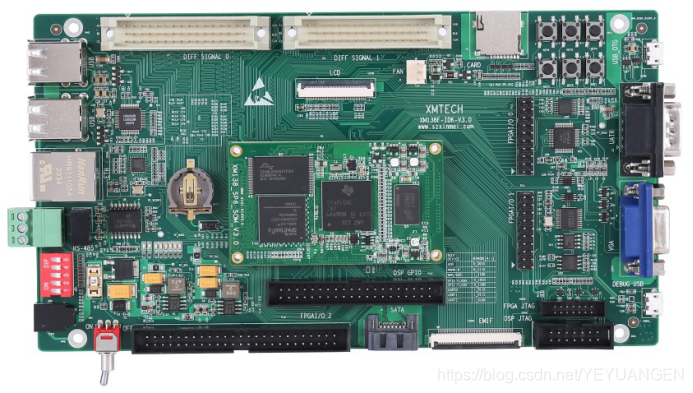 Figure 1 Front and side views of the development board
The XM138F-IDK-V3.0 is a development board designed based on Shenzhen Xinmai's XM138-SP6-SOM core board, featuring a 4-layer board design with immersion gold and lead-free process. It provides users with a test platform for the XM138-SP6-SOM core board to quickly evaluate its overall performance.
The XM138-SP6-SOM exposes all CPU resource signal pins, making secondary development extremely easy. Customers only need to focus on upper-layer applications, significantly reducing development difficulty and time costs, enabling rapid product launch and timely capture of market opportunities. It not only provides rich demo programs but also detailed development tutorials and comprehensive technical support to assist customers with baseboard design, debugging, and software development.
2 Typical Application Areas
- Data acquisition, processing, and display systems
- Smart power systems
- Image processing equipment
- High-precision instrumentation
- Mid-to-high-end CNC systems
- Communication equipment
- Audio and video data processing
 Figure 2 Typical application areas
3 Hardware and Software Parameters
 Schematic diagram of development board peripheral resources
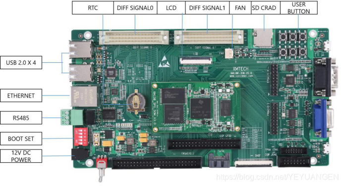
Figure 3 Development board interface schematic
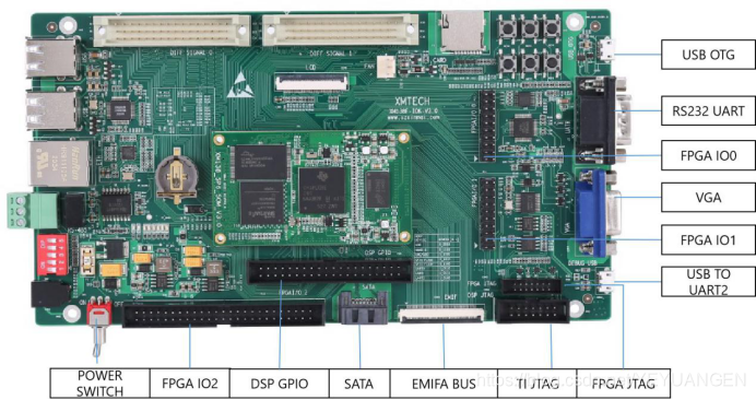
Figure 4 Development board interface schematic
