Design and Application of a Multi-channel PWM Generator Based on OMAPL138+FPGA
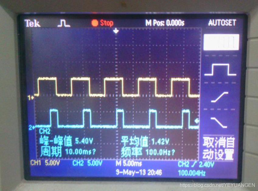
To meet the triggering requirements of inverters in power electronic conversion devices for new energy generation, a multi-channel PWM pulse generator implemented using OMAPL138 and FPGA was developed. This pulse generator uses an interface unit to receive data such as PWM pulse duty cycle and configuration parameters written by the OMAPL138, and uses the FPGA to generate PWM waveforms, achieving operation independent of the OMAPL138. The hardware architecture, basic principles, and implementation methods of the pulse generator are also introduced, and validated through simulation and experiments. This PWM generator not only simplifies circuit design and improves system reliability but also ensures synchronous triggering of inverter power components.
1 Evaluation Board Introduction Based on TI OMAP-L138 (fixed-point/floating-point DSP C674x + ARM9) + Xilinx Spartan-6 FPGA processor; OMAP-L138 and FPGA are connected via uPP, EMIFA, and I2C buses, with communication speeds up to 228 MByte/s; OMAP-L138 has a main frequency of 456MHz, offering computing power up to 3648 MIPS and 2746 MFLOPS; FPGA is compatible with Xilinx Spartan-6 XC6SLX9/16/25/45, providing strong platform upgrade capability; The development board provides rich peripheral interfaces, including high-speed data transfer interfaces such as Gigabit Ethernet, SATA, EMIFA, uPP, USB 2.0, as well as common interfaces like GPIO, I2C, RS232, PWM, and McBSP; Certified through high and low-temperature tests, suitable for various harsh working environments; DSP+ARM+FPGA triple-core SOM (System-on-Module), with dimensions of 66mm*38.6mm, using industrial-grade B2B connectors to ensure signal integrity; Supports bare-metal, SYS/BIOS operating system, and Linux operating system.
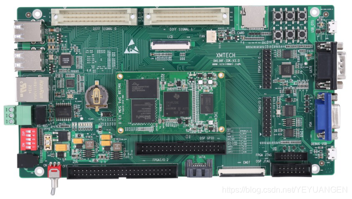 Figure 1 Front and Side Views of the Development Board
The XM138F-IDK-V3.0 is a development board designed based on Shenzhen Xinmai's XM138-SP6-SOM core board. It features a 4-layer board design using immersion gold and lead-free processes. It provides users with a test platform for the XM138-SP6-SOM core board, enabling rapid evaluation of its overall performance.
The XM138-SP6-SOM exposes all CPU resource signal pins, making secondary development extremely easy. Customers only need to focus on upper-layer applications, significantly reducing development difficulty and time costs, enabling rapid product launch and timely capture of market opportunities. It not only provides rich demo programs but also detailed development tutorials and comprehensive technical support to assist customers with baseboard design, debugging, and software development.
2 Typical Application Areas Data Acquisition, Processing, and Display Systems Smart Power Systems Image Processing Equipment High-Precision Instrumentation Mid-to-High-End CNC Systems Communication Equipment Audio and Video Data Processing
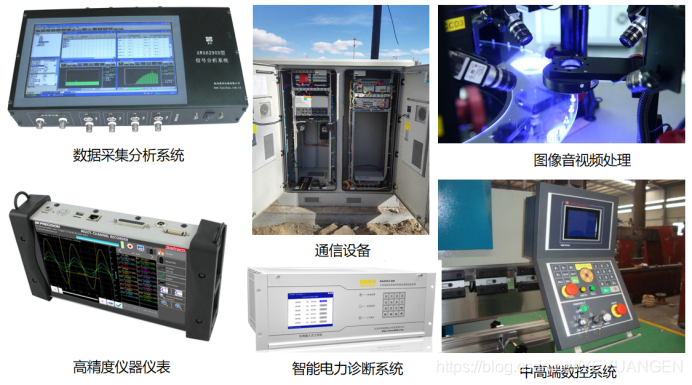 Figure 2 Typical Application Areas
3 Hardware and Software Parameters Development Board Peripheral Resource Block Diagram
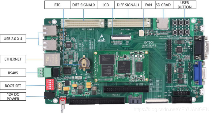
Figure 3 Development Board Interface Diagram
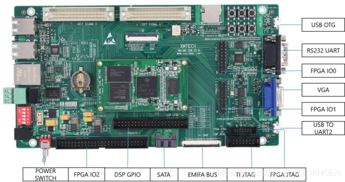
Figure 4 Development Board Interface Diagram