Power Data Acquisition and Transmission Design Based on OMAPL138 + Xilinx Spartan-6
Ma Shixi and Yang Han, researchers from Wuhan Fiberhome Furi Electric Co., Ltd., presented in the 10th issue of "Electrical Engineering" magazine in 2015 a power data acquisition and transmission design based on OMAPL138. This solution is built upon X-Signal’s OMAPL138+SPARTAN6 development board, with the OMAPL138 microprocessor at its core. The microprocessor analyzes and processes acquired data such as voltage, current, and digital inputs, then transmits the processed data to upper-level host systems via interfaces like RS485/RS232 and Ethernet using various communication protocols. The article details the functions of each module, hardware design, and software design flow. This design is flexible, convenient, and offers significant practical value.
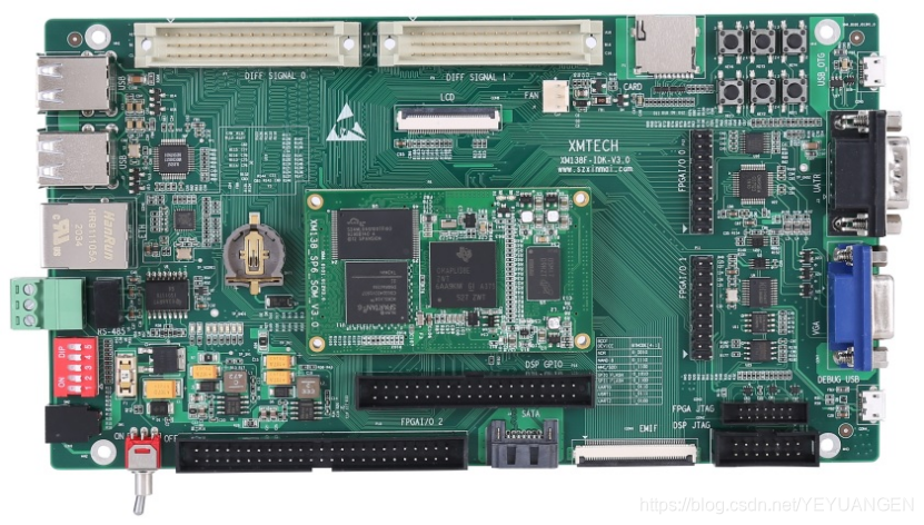
1 Evaluation Board Overview
- Based on TI OMAP-L138 (fixed/floating-point DSP C674x + ARM9) + Xilinx Spartan-6 FPGA processor;
- OMAP-L138 and FPGA are connected via uPP, EMIFA, and I2C buses, supporting communication speeds up to 228 MByte/s; OMAP-L138 operates at a main frequency of 456 MHz, delivering up to 3648 MIPS and 2746 MFLOPS computing performance;
- FPGA compatible with Xilinx Spartan-6 XC6SLX9/16/25/45, offering strong platform scalability;
- The development board exposes rich peripherals, including Gigabit Ethernet, SATA, EMIFA, uPP, USB 2.0, and other high-speed data transmission interfaces, as well as common interfaces such as GPIO, I2C, RS232, PWM, and McBSP;
- Passed high and low-temperature testing certification, suitable for harsh operating environments;
- Triple-core (DSP+ARM+FPGA) core board measuring 66mm × 38.6mm, using industrial-grade B2B connectors to ensure signal integrity;
- Supports bare-metal, SYS/BIOS, and Linux operating systems.
In power system operations, large volumes of data from electrical equipment—such as three-phase voltages, three-phase currents, and switch status signals—must be collected and transmitted over long distances. As power systems continue to evolve, increasingly higher demands are placed on the accuracy of data acquisition and the timeliness of data transmission[1].
Traditional low-end measurement instruments based on microcontrollers suffer from poor data processing capabilities and limited module functionality. Mid-to-high-end instruments based on DSPs take advantage of DSPs' strong data processing performance but often lack sufficient storage capacity and communication capabilities.
Since the International Electrotechnical Commission (IEC) adopted IEC61850 as the standard protocol for seamless communication in power systems in 2000, IEC61850 has gradually been applied in power systems and substation automation both domestically and internationally[2]. However, many existing meters and automated monitoring devices still fail to meet IEC61850 requirements. In practice, both Modbus and IEC61850 protocols often coexist, and devices supporting only a single protocol face significant limitations in application.
To address this issue, this paper proposes a data acquisition and transmission device design based on OMAPL138 that supports multiple communication protocols. The proposed solution can simultaneously support two different protocols, offering flexibility, convenience, and high practical value.
1 Overall Design
The hardware design is based on the OMAPL138 processor, a dual-core embedded microprocessor combining ARM and DSP, developed by Texas Instruments. It features rich peripheral interfaces, including DDR2 controller, Ethernet controller, UARTs, SPI, I2C, LCD controller, USB, and others[3].
The FPGA is compatible with Xilinx Spartan-6 XC6SLX9/16/25/45, enabling strong platform upgrade capability. The use of an OMAPL138+SPARTAN6 core board facilitates secondary development.
In this design, the OMAPL138 microprocessor connects to Nand-Flash via the EMIFA bus. The Nand-Flash stores UBOOT, the operating system kernel, file system, application programs, and related data. OMAPL138 connects to a DDR2SDRAM chip via the DDR2 bus, which is used for running the operating system and applications and storing temporary files.
As shown in Figure 1, OMAPL138 connects to an external analog-to-digital converter (ADC) via the SPI interface to acquire analog signals. It uses universal asynchronous serial ports (UARTs) to multiplex between RS232 and RS485 modes, transmitting acquired data using the Modbus protocol from the acquisition terminal to the backend system.
OMAPL138 connects its internal Ethernet controller to an external Ethernet PHY chip via the MII interface, enabling Ethernet communication. Collected data is sent to the backend using the IEC61850 protocol over the Ethernet interface.
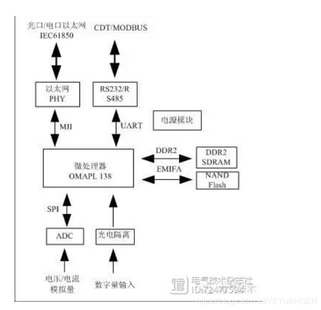
Figure 1 Hardware System Block Diagram
2 Hardware Design
2.1 Acquisition Module Design
- Analog Input Acquisition Module
The design uses ADI's AD7689 as the analog-to-digital converter, which features 8 analog input channels, 16-bit resolution, and a sampling rate of 250 kSPS[4]. The AD7689 converts analog signals into digital form and sends the digitized data to the processor via the SPI bus for further processing.
Configuration in this design is as follows: (1) The ADC is powered by 5V, with a reference voltage of 4.096V provided by an internal voltage reference; (2) The ADC's digital output voltage is 3.3V, matching the processor's IO voltage level; (3) The analog input signals are unipolar, converted from differential signals from current/voltage transformers via a signal conditioning circuit; (4) The data output rate is controlled by the processor.
- Digital Input Acquisition Module
Digital input signals (switch status) are optically isolated and then directly fed into the IO pins of the OMAPL138 processor. Software configures these IO pins as inputs to capture external digital signals, which are then stored in shared memory and subsequently transmitted using the appropriate communication protocol.
2.2 Communication Module Design
The design supports both Modbus and IEC61850 protocols, enabling flexible adaptation to different communication requirements. Modbus can be implemented via either RS232 or RS485, with software-configurable multiplexing and automatic switching between the two. IEC61850 communication uses either optical or electrical Ethernet interfaces.
- RS232/RS485 Multiplexed Interface
The circuit diagram for the RS232/RS485 multiplexing scheme is shown in Figure 2. The OMAPL138 UART's transmit pin connects to both the transmit input of the RS232 module (MAX3232) and the transmit input of the RS485 module (MAX485). Similarly, the UART's receive pin connects to both the receive output of MAX3232 and MAX485.
Two IO pins of OMAPL138 drive the set and reset coils of a dual-coil latching miniature relay. Pulse signals on these IO pins switch the relay contacts between set and reset states.
To enhance the driving capability of the OMAPL138 IO pins, this design uses the IO pins to drive transistors, which in turn drive the relays. This allows the processor to control which interface—RS232 or RS485—is connected to the external communication lines by changing the state of its IO pins. Thus, the two communication methods can be easily multiplexed through software configuration.
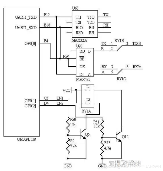
Figure 2 RS232/RS485 Multiplexed Communication Module
- Ethernet Communication Interface Design
The OMAPL138 processor includes an Ethernet controller supporting 10/100 Mbps Ethernet. By connecting its MII or RMII interface to an external Ethernet PHY chip, Ethernet communication is achieved. This design uses Micrel's KSZ8001 as the Ethernet PHY chip, supporting both optical and electrical 10/100 Mbps Ethernet. The circuit diagram for the OMAPL138 and KSZ8001 Ethernet interface is shown in Figure 3.
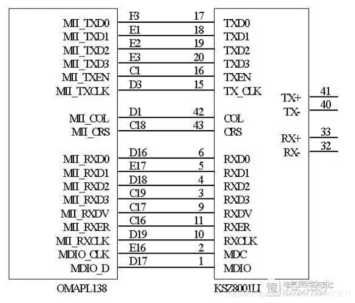
Figure 3 Ethernet Communication Interface Circuit Diagram
2.3 Power Supply Design
The design requires three power supply voltages: 1.2V, 1.8V, and 3.3V, which are used for the processor core, DDR2 controller, processor IO, and other chip operations, respectively. These voltages are generated from an external 5V supply using dedicated power management ICs: Intersil's ISL6410A and ISL65426. ISL6410A provides 1.2V output, while ISL65426 provides 1.8V and 3.3V outputs.
ISL6410A and ISL65426 are high-performance PWM-modulated DC/DC converters from Intersil, capable of delivering stable voltage and current output across an industrial temperature range of -40°C to 85°C with high conversion efficiency[5][6].
Both chips integrate internal MOSFETs and include properly designed power-good and enable pins, greatly simplifying user design.
When designing the power supply with these ICs, the following points should be noted:
(1) Since the OMAPL138 processor has specific power-up sequencing requirements, it is essential that 1.2V is established before 1.8V, and 1.8V before 3.3V. The enable pin (EN) of ISL6410A is pulled up to 5V. Its power-good pin (PG) is connected to the enable pin (EN1) of the 1.8V output channel of ISL65426. The power-good pin (PG1) of the 1.8V output channel is connected to the enable pin (EN2) of the 3.3V output channel. This ensures proper power-up sequencing.
(2) The output configuration pin (VSET) of ISL6410A is pulled up to 5V, ensuring that ISL6410A correctly outputs 1.2V when supplied with 5V input.
(3) ISL65426 has two output channels and six adjustable power output modules, allowing independent configuration. Output voltages can be set via programming pins; for non-standard voltages, feedback via resistive dividers can be used. Since 1.8V and 3.3V are supported by programming pins in this design, pins V1SET1, V1SET2, V2SET1, and V2SET2 are all pulled up to 5V. Given that the 3.3V supply draws more current than the 1.8V supply in this design, the current configuration pins ISET1 and ISET2 are set to 1 and 0, respectively.
3 Software Design
The software consists of five components: ubl, uboot, Linux kernel, file system, and application programs. The ubl and uboot handle initialization of OMAPL138 and loading/launching the kernel.
The Linux kernel version used is 2.6.32, extended with custom serial port drivers. The application layer supports multiple communication protocols, including ModbusRTU and IEC61850 for data reporting. After processing the acquired signals using algorithms, the CPU writes the results into shared memory for use by various protocol modules in packet encapsulation.
3.1 Low-Level Serial Port Driver
The Modbus protocol is supported via serial communication with upper-level devices. Serial data transmission and reception are handled by kernel-level serial drivers. The Linux serial driver architecture comprises three layers: low-level driver, line discipline, and tty device driver core, as illustrated in Figure 4.
As shown in Figure 4, user-space commands and data are passed to the low-level driver, processed and scheduled by the line discipline, and then passed to the tty core layer, which performs hardware operations according to the command. In some cases, data may bypass the line discipline and go directly from the low-level driver to the core driver.
3.2 Data Acquisition and Processing
- Data Accuracy Algorithm
To minimize anomalies in A/D acquisition data caused by environmental interference or hardware issues, the design applies algorithmic processing before storing data in shared memory. The algorithm discards the highest and lowest values from ten consecutive samples and computes the average of the remaining eight values as the valid signal for that acquisition cycle. While this reduces data acquisition efficiency, it improves data reliability and is suitable for applications where high sampling rates are not critical.
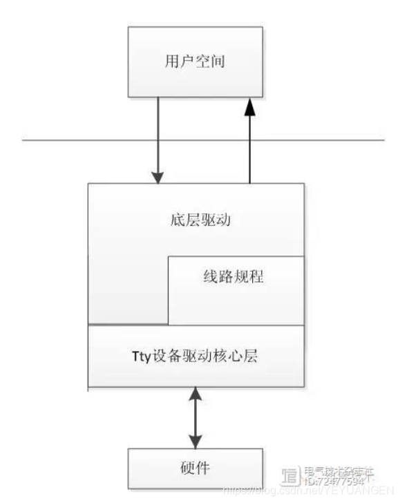
Figure 4 Serial Port Driver Architecture
- Data Transfer
To ensure efficient data transfer between protocols, this design uses shared memory. The data structures for different protocols map to the same physical memory block. During main process startup, a memory block is allocated. The configuration file is then read to define the mapping of data structure members across protocols, enabling seamless inter-protocol data sharing.
3.3 Communication Protocols
The design supports the ModbusRTU protocol, acting as a slave device that responds to various operations initiated by upper-level devices via ModbusRTU. Communication with upper-level devices occurs via either RS485 or RS232, with the interface type selectable via configuration file. Considering the half-duplex nature of RS485, appropriate delays are introduced between sending and receiving to ensure data integrity.
The system also supports the IEC61850 protocol, transmitting data to the backend via Ethernet. Data for both protocols originates from shared memory. The system module block diagram is shown in Figure 5. As seen in Figure 5, both protocol modules operate as independent task processes, allowing the system to simultaneously support both protocols and serve multiple types of upper-level devices.
3.4 Data Logging
The design includes comprehensive fault logging, saving abnormal operational data and fault timestamps to log files stored in flash memory for easy troubleshooting by maintenance personnel. Additionally, historical data logging is supported, recording each data change along with its timestamp into log files stored in flash. The system supports up to 128MB of log file storage.
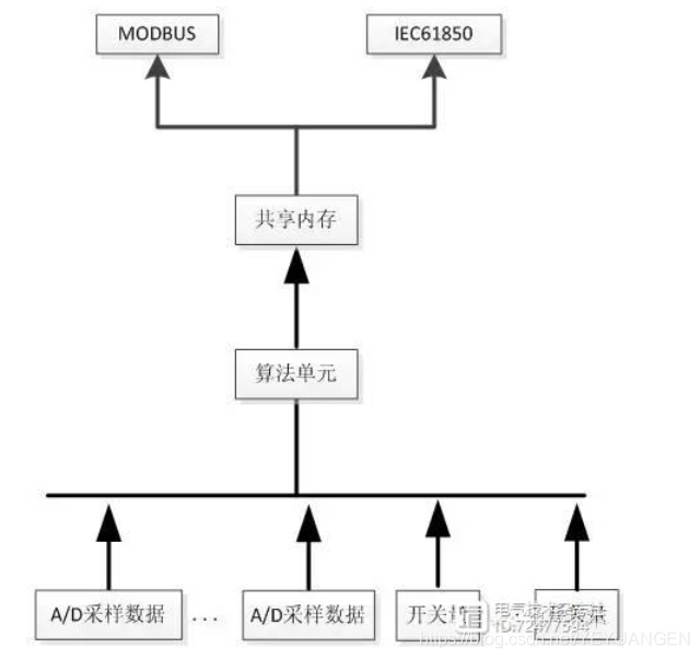
Figure 5 Data Acquisition and Shared Memory Module Diagram
4 Testing and Verification
To verify the data acquisition functionality and the Modbus and IEC61850 communication capabilities, the following test setup was used: A relay protection tester outputs three-phase current, three-phase voltage, and digital signals to the device under test. The device acquires and processes the data, then transmits it to a PC using both Modbus and IEC61850 protocols.
For Modbus communication verification, the PC sends Modbus polling messages to the device via a serial debugging tool and checks the response data.
IEC61850 communication is verified using the Ethernet packet capture tool MMS Ethereal to capture MMS messages and inspect data transmission. Screenshots of the transmitted protocol messages are shown in Figures 6 and 7. Comparison of the protocol messages with the data output from the relay protection tester confirms that the design meets the original requirements.
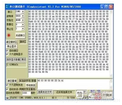
Figure 6 Modbus Polling and Response
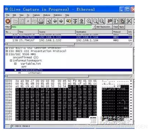
Figure 7 MMS Message
5 Conclusion
This paper presents a power data acquisition and multi-protocol transmission solution based on OMAPL138. The modular design supports multiple communication protocols for data transmission, greatly enhancing user convenience. It also provides a robust hardware and software platform for future expansion of additional functionalities and protocols, demonstrating high practical value.