Research and Implementation of a Reactive Power Compensation System Structure for a Static Synchronous Compensator Based on OMAPL138+FPGA
The increasing variety of nonlinear devices in power systems impacts the power supply, leading to significant fluctuations in supply voltage amplitude, reduced power factor, and increased harmonic distortion in the public grid. Simultaneously, with the rapid development of computer technology and precision control, user demands for power quality are also rising. This energy contradiction has accelerated the theoretical research and engineering application of reactive power compensation technology in power systems. Thanks to the comprehensive improvement in switching device performance, the regulation effect of reactive power compensation devices has become increasingly outstanding. Compared with similar reactive power compensation devices, Static Synchronous Compensator (STATCOM) systems offer advantages such as low harmonics, a wide dynamic adjustment range, and high reliability. Therefore, research into STATCOM control systems, as presented in this paper, holds significant value. This paper takes a grid-connected STATCOM device as a reference model and develops a generalized cascaded STATCOM hardware device for three-phase 220V AC power. It then implements the control strategy software based on an OMAPL138 and FPGA operating platform. In terms of hardware design, this paper uses OMAPL138 and XC6SLX16 as the main system processors and adopts a modular hardware design structure based on system functions. This constructs a STATCOM system hardware platform comprising a CPU module, signal input/output module, and drive signal control module. To facilitate flexible addition or removal of functional modules by users according to application requirements, the device's hardware structure employs a mother-daughter board plug-in method. In terms of software design, based on the cascaded STATCOM mathematical model and the energy flow relationship of the system circuit, this paper adopts a hierarchical structure. It designs a control algorithm system primarily consisting of inner-loop decoupled control, active and reactive current control, and cascaded unit voltage balancing control, based on the decoupled equations of STATCOM system current and voltage. Simultaneously, to cope with the strong electromagnetic interference environment in which STATCOM systems operate, this paper addresses circuit design, PCB layout and routing, and interference sources to improve the system's anti-interference capability and ensure the reliability of transmitted signals. The anti-interference performance of the STATCOM device is verified through EMC testing. Finally, a four-cascaded H-bridge STATCOM system is built using MATLAB, and the control strategy adopted in this paper is verified in a SIMULINK simulation model. On this basis, combining STATCOM system simulation and the hardware platform, an experimental approach from local to global is adopted. Experiments on the system's reactive power compensation performance are conducted, starting with the sampling of system current and voltage signals and the isolation and amplification of cascaded drive signals. Experimental results show that the cascaded STATCOM hardware device designed in this paper operates stably and reliably in practical applications and effectively achieves reactive power compensation for three-phase 220V AC power.
1 Evaluation Board Introduction
- Based on TI OMAP-L138 (fixed-point/floating-point DSP C674x + ARM9) + Xilinx Spartan-6 FPGA processor;
- OMAP-L138 and FPGA are connected via uPP, EMIFA, and I2C buses, with communication speeds up to 228 MByte/s; OMAP-L138 has a main frequency of 456MHz, with computing power up to 3648 MIPS and 2746 MFLOPS;
- FPGA is compatible with Xilinx Spartan-6 XC6SLX9/16/25/45, offering strong platform upgrade capabilities;
- The development board provides rich peripheral interfaces, including Gigabit Ethernet, SATA, EMIFA, uPP, USB 2.0 and other high-speed data transmission interfaces, as well as common interfaces such as GPIO, I2C, RS232, PWM, and McBSP;
- Certified through high and low-temperature testing, suitable for various harsh working environments;
- DSP+ARM+FPGA triple-core SOM, with dimensions of 66mm*38.6mm, using industrial-grade B2B connectors to ensure signal integrity; Ø
- Supports bare-metal, SYS/BIOS operating system, and Linux operating system.
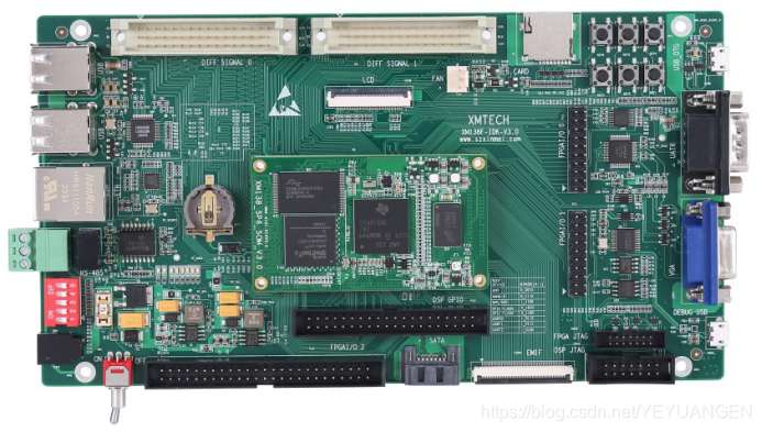
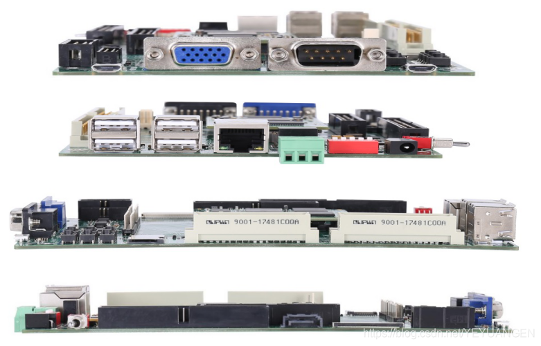 Figure 1 Front and side views of the development board
The XM138F-IDK-V3.0 is a development board designed based on Shenzhen Xinmai's XM138-SP6-SOM core board. It features a 4-layer board design with immersion gold lead-free process, providing users with a test platform for the XM138-SP6-SOM core board to quickly evaluate its overall performance.
The XM138-SP6-SOM exposes all CPU resource signal pins, making secondary development extremely easy. Customers only need to focus on the upper-layer application, greatly reducing development difficulty and time costs, allowing products to be launched quickly and seize market opportunities. It not only provides rich demo programs but also detailed development tutorials, comprehensive technical support, assisting customers with baseboard design, debugging, and software development.
2 Typical Application Areas Data acquisition, processing, and display systems Smart power systems Image processing equipment High-precision instrumentation Mid-to-high-end CNC systems Communication equipment Audio and video data processing
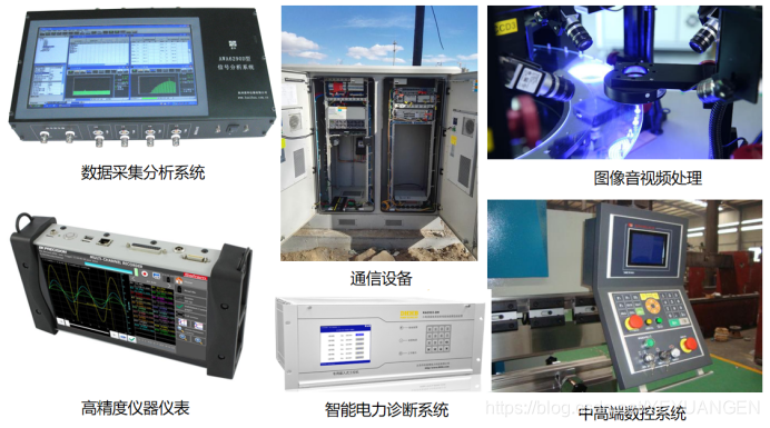 Figure 2 Typical application areas