Impressions from Testing the C6748 + SPARTAN6 Core Board and Evaluation Board
Last week, I acquired the C6748 + SPARTAN6 development board from Shenzhen Xinmingxin Technology. My first impression was that the core board is incredibly compact—about the size of a coin. It uses three DC-DC converters for power, resulting in low power consumption, and all chips are industrial-grade, making it highly suitable for our power monitoring equipment.
One notable feature is that the board includes EMC and ESD protection, eliminating concerns about electromagnetic interference in power systems.
After spending a week experimenting with the example programs they provided, I found the Qt integration particularly impressive. Here are a few photos I found online for reference.
1. Evaluation Board Overview
- Based on the TI TMS320C6748 fixed-point/floating-point DSP C674x and Xilinx Spartan-6 FPGA processor;
Ø DSP and FPGA are connected via uPP, EMIFA, and I2C buses, supporting communication speeds up to 228 MByte/s;
Ø DSP clocked at 456 MHz, delivering up to 3648 MIPS and 2746 MFLOPS computing performance; - FPGA compatible with Xilinx Spartan-6 XC6SLX9/16/25/45, enabling strong platform scalability;
- The development board exposes abundant peripherals, including Gigabit Ethernet, SATA, EMIFA, uPP, and USB 2.0 for high-speed data transmission, as well as common interfaces such as GPIO, I2C, RS232, PWM, McBSP, VGA, PMOD, and RS485;
- Certified for high and low temperature operation, suitable for harsh working environments;
- DSP + FPGA dual-core core board measuring 66mm × 38.6mm, using industrial-grade B2B connectors to ensure signal integrity;
Ø - Integrated charge/discharge battery circuitry, multiple standard industrial interfaces, supports connection to multi-channel AD/DA modules, offering strong expandability;
- Supports bare-metal and SYS/BIOS operating systems.
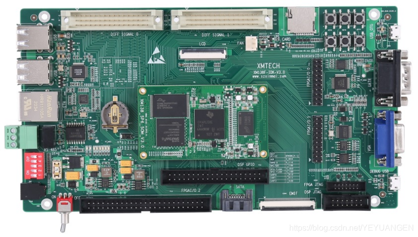
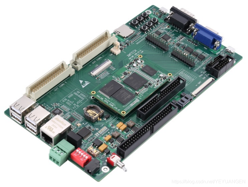
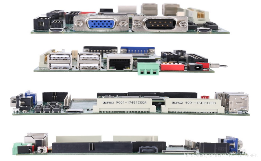
Figure 1: Front and side views of the development board
The XM6748F-IDK-V3.0 is a development board designed around the Shenzhen Xinmingxin XM6748F-SOM core module. It features a 4-layer PCB with lead-free immersion gold finish and serves as a testing platform for the XM6748F-SOM core board, enabling rapid evaluation of its overall performance.
The XM6748F-SOM exposes all CPU resource signal pins, making secondary development extremely easy. Customers can focus solely on application-level development, significantly reducing development difficulty and time-to-market, allowing products to launch quickly and seize market opportunities. In addition to rich demo programs, detailed development tutorials and comprehensive technical support are provided to assist customers with carrier board design, debugging, and software development.
2. Typical Application Areas
- Data acquisition, processing, and display systems
- Intelligent power systems
- Image processing equipment
- High-precision instruments and meters
- Mid-to-high-end CNC systems
- Communication equipment
- Audio and video data processing
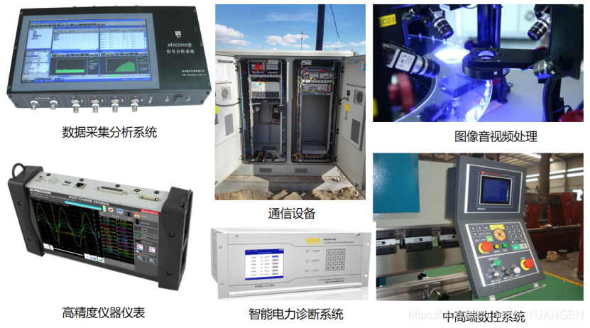
Figure 2: Typical application areas
3. Hardware and Software Specifications
Peripheral resource block diagram of the development board
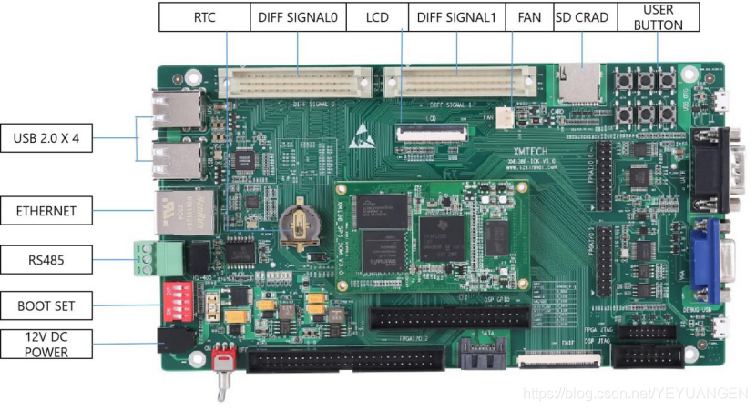
Figure 3: Development board interface diagram
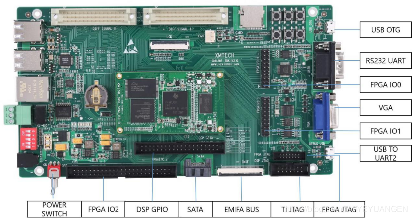
Figure 4: Development board interface diagram
Table 1: Hardware Resources
CPU
TI TMS320C6748, fixed-point/floating-point DSP C674x, 456 MHz
Xilinx Spartan-6 XC6SLX9/16/25/45 FPGA
ROM
TMS320C6748 side: 128/256/512 MByte NAND FLASH
Spartan-6 side: 64 Mbit SPI FLASH
RAM
TMS320C6748 side: 128/256 MByte DDR2
B2B Connector
2×80-pin male B2B, 2×80-pin female B2B, 0.5 mm pitch, total 320 pins
IO
2×25-pin IDC3 header, 2.54 mm pitch, EMIFA expansion signals
2×25-pin IDC3 header, 2.54 mm pitch, FPGA GPIO expansion signals
2×15-pin headers, 2.54 mm pitch, including I2C, McBSP, PWM, FPGA differential IO, and other expansion signals
LED
2× power indicator LEDs (1 on baseboard, 1 on core board)
5× programmable LEDs (3 on baseboard, 2 on core board)
5× programmable LEDs (3 on baseboard, 2 on core board, FPGA side)
KEY
1× system reset button
3× programmable input buttons (including 1 non-maskable interrupt button)
5× programmable LEDs (3 on baseboard, 2 on core board, FPGA side)
JTAG
1× 14-pin TI Rev B JTAG interface, 2.54 mm pitch
1× 14-pin FPGA JTAG interface, 2.00 mm pitch
LCD
1× LCD touchscreen interface
BOOT SET
1× 5-bit DIP switch for boot mode selection
SD
1× Micro SD card interface
RTC
1× RC1220 RTC socket, 3V
SATA
1× 7-pin SATA hard drive interface
Ethernet
1× RJ45 Ethernet port, 10/100M auto-negotiation
USB
1× Micro USB 2.0 OTG interface
1× USB 1.1 HOST interface
UART
2× RS232 serial ports: UART2 via Micro USB, UART1 via DB9; 4-wire TTL header (TXD, RXD, 3V3, GND) also exposed
SWITCH
1× power toggle switch
POWER
1× 12V 2A DC input via DC417 connector, 4.4 mm outer diameter, 1.65 mm inner diameter
Note: Shenzhen Xinmingxin's XM138F-SOM, XM1808F-SOM, and XM6748F-SOM core boards are pin-to-pin compatible in hardware.
Table 2: Software Resources
DSP Software Support
Bare-metal, SYS/BIOS operating system
CCS Version
CCS 5.5
ISE Version
ISE 14.7
4. Development Resources
(1) Provide core board pin definitions, editable carrier board schematics and PCB files, and chip datasheets to shorten hardware design cycles;
(2) Provide system flashing images, kernel driver source code, file system source code, and a rich set of demo programs;
(3) Provide complete platform development packages and getting-started tutorials to save software setup time and ease onboarding;
(4) Provide extensive tutorials and development examples, including OMAP-L138 and FPGA communication examples;
(5) Provide detailed DSP + ARM dual-core communication tutorials to effectively overcome dual-core development bottlenecks;
(6) Provide Qt-based graphical interface development tutorials.
Shenzhen Xinmingxin offers extensive development materials, video tutorials, and Chinese datasheets, setting a new benchmark for OMAP-L138 platform development and driving widespread interest in the OMAP-L138 + Spartan-6 DSP + ARM + FPGA tri-core architecture.
See Appendix A for selected development examples, including:
- Bare-metal development examples for ARM side
- Linux development examples for ARM side
- Bare-metal development examples for DSP side
- SYS/BIOS development examples for DSP side
- SYSLINK-based dual-core development examples
- DSPLINK-based dual-core development examples
- XM_IPC-based dual-core development examples
- PRU assembly development examples
- FPGA-side development examples
5. Electrical Characteristics
Core Board Operating Environment
Table 3
Environmental Parameter
Minimum
Typical
Maximum
Commercial Temperature
0°C
/
70°C
Industrial Temperature
-40°C
/
85°C
Operating Voltage
/
3.3V
/
Power Consumption Test
Table 4
Category
Typical Voltage
Typical Current
Typical Power
Core Board
3.3V
74 mA
0.24 W
Full Board
12.01 V
100 mA
1.20 W
Note: Power consumption test conducted on Shenzhen Xinmingxin XM6748F-IDK-V3 development board.
6. Mechanical Dimensions
Table 5
Core Board
Development Board
PCB Dimensions
66mm × 38.6mm
165mm × 110mm
Number of Mounting Holes
4
12
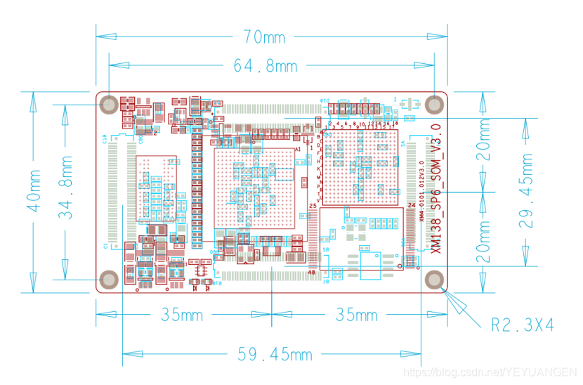
Figure 5: Core board mechanical dimensions
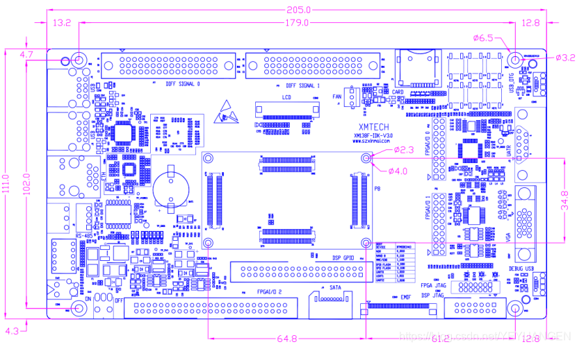
Figure 6: Evaluation board mechanical dimensions
7. Product Ordering Models
Table 6
Model
CPU Frequency
NAND FLASH
DDR2
SPI FLASH
FPGA Model
Temperature Grade
SOM-XM6748F-4-4GN1GD2S16-I
456 MHz
512 MB
128 MB
64 Mbit
XC6SLX16
Industrial
SOM-XM6748F-4-4GN2GD2S16-I
456 MHz
512 MB
256 MB
64 Mbit
XC6SLX16
Industrial
SOM-XM6748F-4-4GN1GD2S45-I
456 MHz
512 MB
128 MB
64 Mbit
XC6SLX45
Industrial
SOM-XM6748F-4-4GN2GD2S45-I
456 MHz
512 MB
256 MB
64 Mbit
XC6SLX45
Industrial
Note: Default configuration is SOM-XM6748F-4-4GN1GD2S16-I. Contact sales for other models.
8. Development Board Kit Contents
Table 7
Item
Quantity
XM6748F-IDK-V3 Development Board (with core board)
1 unit
12V/2A Power Adapter
1 unit
Documentation CD
1 set
Micro SD System Card
1 unit
SD Card Reader
1 unit
Straight Ethernet Cable
1 piece
Micro USB Data Cable
1 piece
9. Technical Support
(1) Assist with carrier board design and testing to reduce hardware design errors;
(2) Help resolve anomalies encountered during operation per user manual;
(3) Assist in product fault diagnosis;
(4) Help correctly compile and run provided source code;
(5) Support secondary product development;
(6) Provide long-term after-sales service.
10. Value-Added Services
- Custom carrier board design
- Custom core board design
- Embedded software development
- Joint project development
- Technical training