Design and Implementation of an OMAPL138+FPGA-based RF Direct Sampling Weather Facsimile Receiver
Weather facsimile signals cover most of the world's oceans. By receiving weather charts via a weather facsimile receiver, ships in the open ocean can timely predict dangerous factors such as typhoons and high waves that threaten navigation safety, allowing them to plan or alter their routes accordingly. The weather information received by facsimile machines is of significant importance for the safety and route selection of ships. Most weather facsimile machines currently in use employ a superheterodyne architecture, which involves complex analog signal processing, makes fault detection difficult, and has low digital integration. Addressing the pros and cons of existing receiver structures, this paper proposes a design for an RF direct sampling weather facsimile receiver based on software-defined radio principles.
With this solution, RF signals are directly digitized after sampling, eliminating the need for analog demodulation. This reduces the size, simplifies the RF front-end design, improves system integration, and lowers the risk of faults caused by analog signal processing. The RF direct sampling weather facsimile receiver primarily consists of three parts: the RF front-end module, the A/D sampling and digital down-conversion module, and the system control and data processing module. Specifically, the RF front-end module comprises an antenna matching and protection circuit, a frequency-selective bandpass filter circuit, a high-frequency amplification and automatic gain amplification circuit, and a front-end control circuit. The A/D sampling and digital down-conversion module consists of an anti-aliasing filter and signal conditioning circuit, an analog-to-digital converter, and an FPGA. The system control and data processing module is a core board based on the OMAPL138 dual-core processor. The system backplane provides power and peripheral interface circuits for the above modules. The signal processing flow is roughly as follows: RF signals received by the antenna first undergo bandpass filtering and signal amplification in the front-end module. After A/D sampling, digital down-conversion is performed in the FPGA. The FPGA then sends the data to the DSP core for differential detection and demodulation. The DSP transfers the data to the ARM core via a shared memory area. The image data generated by the ARM core is finally uploaded to the host computer interface via Ethernet for display. This paper introduces the RF direct sampling weather facsimile receiver, compares its performance indicators with other receiver architectures, explains the hardware design principles and software design concepts, and based on this, completes a detailed analysis and design of each system module. Finally, through system debugging and result analysis, the correctness of the RF direct sampling design solution is verified.
1 Evaluation Board Introduction
- Based on TI OMAP-L138 (fixed-point/floating-point DSP C674x + ARM9) + Xilinx Spartan-6 FPGA processor;
- OMAP-L138 and FPGA are connected via uPP, EMIFA, and I2C buses, with communication speeds up to 228 MByte/s; OMAP-L138 has a main frequency of 456MHz, with computing power up to 3648 MIPS and 2746 MFLOPS;
- FPGA is compatible with Xilinx Spartan-6 XC6SLX9/16/25/45, offering strong platform upgrade capabilities;
- The development board exposes rich peripherals, including Gigabit Ethernet, SATA, EMIFA, uPP, USB 2.0 and other high-speed data transfer interfaces, as well as common interfaces like GPIO, I2C, RS232, PWM, McBSP;
- Certified through high and low-temperature tests, suitable for various harsh working environments;
- DSP+ARM+FPGA triple-core module, with dimensions of 66mm*38.6mm, using industrial-grade B2B connectors to ensure signal integrity; Ø
- Supports bare-metal, SYS/BIOS operating system, and Linux operating system.
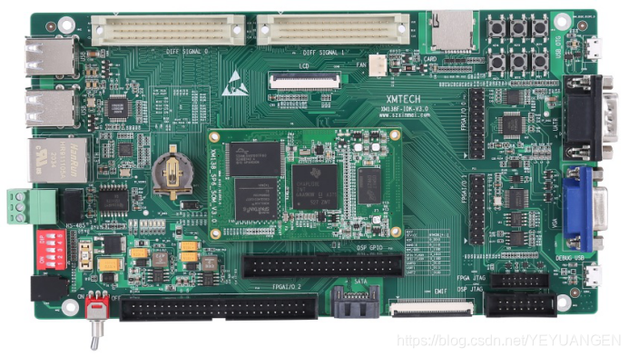
Figure 1 Development Board Front and Side Views
The XM138F-IDK-V3.0 is a development board designed based on Shenzhen Xinmai's XM138-SP6-SOM core board. It features a 4-layer board design with immersion gold lead-free process and provides users with a test platform for the XM138-SP6-SOM core board, enabling quick evaluation of its overall performance.
The XM138-SP6-SOM exposes all CPU resource signal pins, making secondary development extremely easy. Customers only need to focus on the upper-layer applications, greatly reducing development difficulty and time costs, allowing products to quickly enter the market and seize market opportunities. It not only provides rich demo programs but also detailed development tutorials and comprehensive technical support to assist customers with backplane design, debugging, and software development.
2 Typical Application Areas
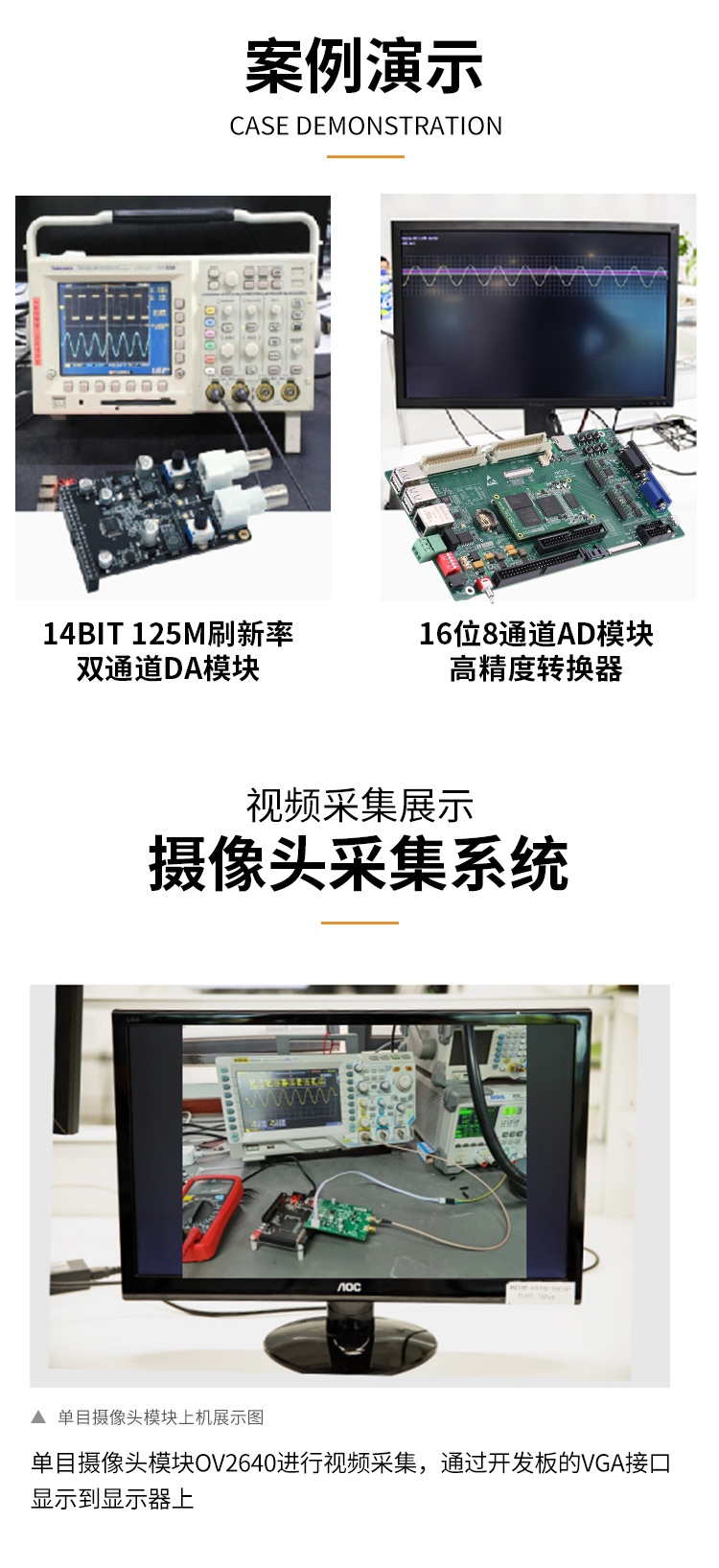
Data acquisition, processing, and display systems
Intelligent power systems
Image processing equipment
High-precision instrumentation
Mid-to-high-end CNC systems
Communication equipment
Audio and video data processing
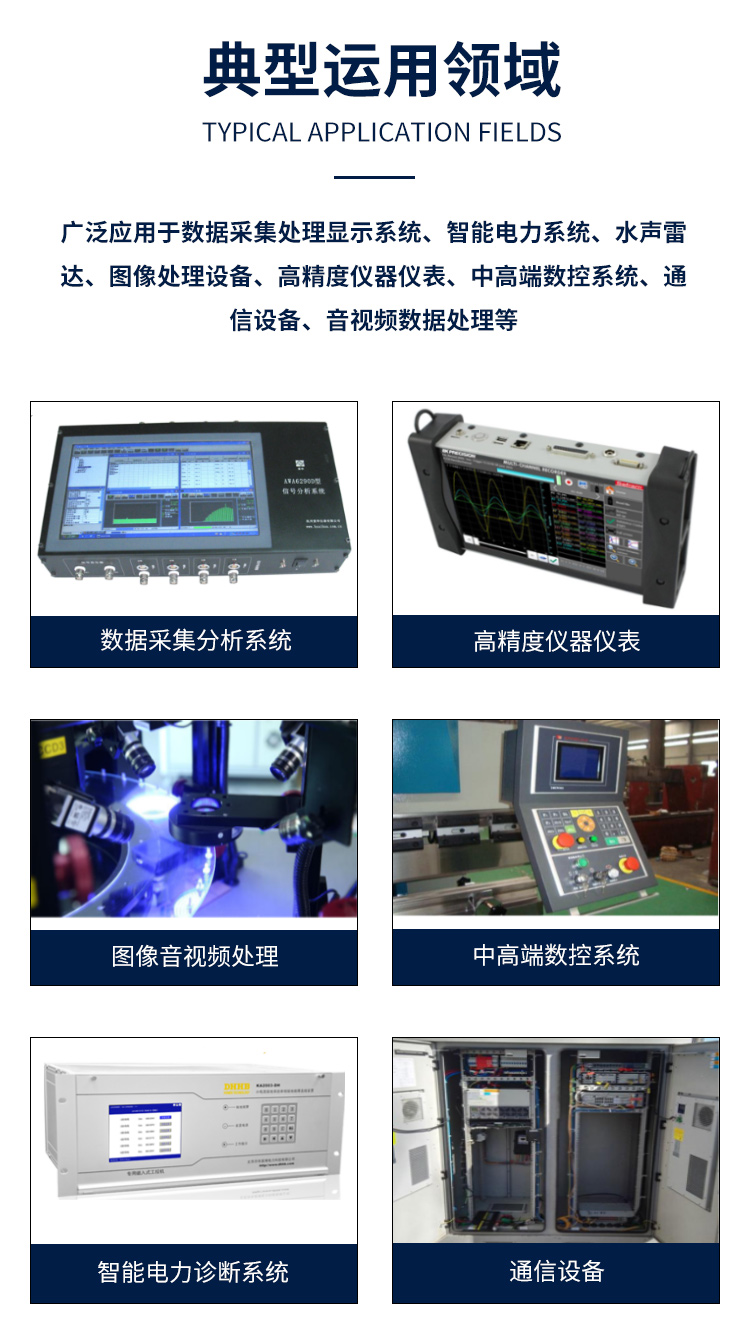
Figure 2 Typical Application Areas
3 Hardware and Software Parameters
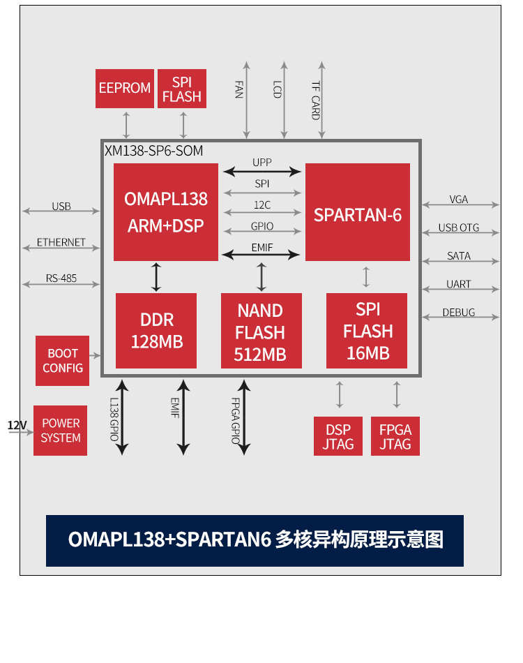
Development Board Peripheral Resource Block Diagram
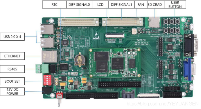
Figure 3 Development Board Interface Diagram
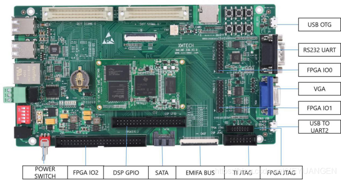
Figure 4 Development Board Interface Diagram