ADCP Signal Processing System Based on C6748 DSP + FPGA Acoustic Doppler Current Profiler
The Acoustic Doppler Current Profiler (ADCP) is a device that measures flow velocities at different depths across a water column by utilizing the Doppler effect of ultrasonic signals and ultrasonic ranging principles. It is widely used in ocean current observation and river discharge measurement. Currently, digital ADCP technology is relatively mature overseas, while there are no commercially available products in China yet. Therefore, it is essential to develop China's own ADCP technology and products. Due to limitations in processor computational performance and power consumption, traditional ADCP algorithms and systems were primarily implemented using analog circuits. With improvements in DSP processing capabilities and in ADC resolution and sampling rates, there is a growing preference to perform signal processing as much as possible in the digital domain. This approach simplifies the analog front-end complexity and enhances the system's versatility, flexibility, and stability. After thorough research and analysis, and based on a solid understanding of the fundamental principles of ADCP technology, the author established the development plan for the ADCP signal processing system described in this paper. The design leverages FPGA technology with high-speed parallel processing capability and powerful DSP signal processing techniques. It employs short-time power spectrum estimation algorithms—specifically, the complex autocorrelation method and the AR power spectrum estimation algorithm. By applying superheterodyne technology, TGA amplification technology, and ultrasonic power driving technology, the system achieves extraction, amplification, and transmission of high-frequency weak signals. Corresponding schematic circuits and PCBs were designed, hardware was fabricated, and computational workflows were established. Software programs were developed accordingly, ultimately completing a benchtop digital ADCP signal processing system in the laboratory. Functional tests under laboratory conditions and simple water environment velocity measurements were conducted on the completed system. Results indicate that the system successfully achieves its intended basic functions. The designed ADCP system features strong functionality, compact size, high cost-effectiveness, simple structure, and excellent versatility. By utilizing FPGA and DSP, the system’s signal acquisition and data processing capabilities are significantly enhanced. This provides an efficient validation platform for research on transducer transmit waveforms and Doppler shift estimation methods in ADCP systems.
1 Evaluation Board Overview
Based on TI OMAP-L138 (fixed/floating-point DSP C674x + ARM9) + Xilinx Spartan-6 FPGA processor;
OMAP-L138 connects to FPGA via uPP, EMIFA, and I2C buses, supporting communication speeds up to 228 MByte/s;
OMAP-L138 operates at a maximum clock rate of 456 MHz, delivering up to 3648 MIPS and 2746 MFLOPS computing performance;
FPGA compatible with Xilinx Spartan-6 XC6SLX9/16/25/45, offering strong platform scalability;
DSP + ARM + FPGA tri-core SOM, sized 66mm × 38.6mm, uses industrial-grade B2B connectors to ensure signal integrity;
Supports bare-metal, SYS/BIOS, and Linux operating systems.
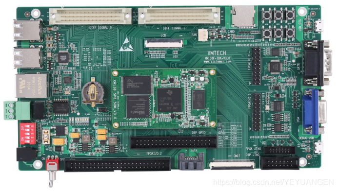
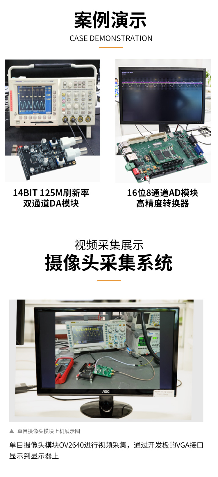
Figure 1: Front and side views of the development board
XM138F-IDK-V3.0 is a development board designed based on the Shenzhen Xinmeng XM138-SP6-SOM system-on-module, fabricated using a 4-layer lead-free immersion gold process. It provides a test platform for the XM138-SP6-SOM, enabling rapid evaluation of the module’s overall performance.
The XM138-SP6-SOM exposes all CPU resource signal pins, making secondary development extremely easy. Customers can focus on application-level development, significantly reducing development difficulty and time cost, accelerating time-to-market and enabling timely capture of market opportunities. In addition to providing rich demo programs, comprehensive development tutorials and full technical support are offered to assist customers with carrier board design, debugging, and software development.
2 Typical Application Areas
Data acquisition, processing, and display systems
Smart power systems
Image processing equipment
High-precision instruments and meters
Mid-to-high-end numerical control systems
Communication equipment
Audio and video data processing
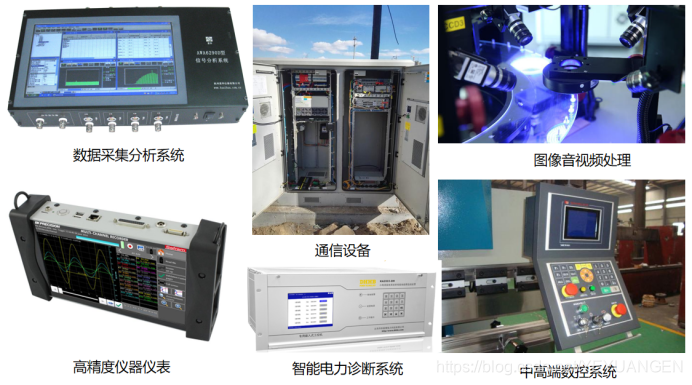
Figure 2: Typical application areas
3 Hardware and Software Specifications
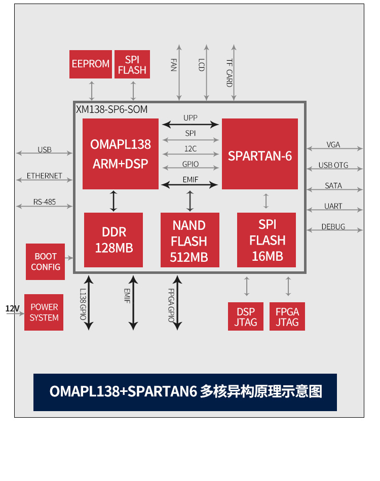
Peripheral resource block diagram of the development board
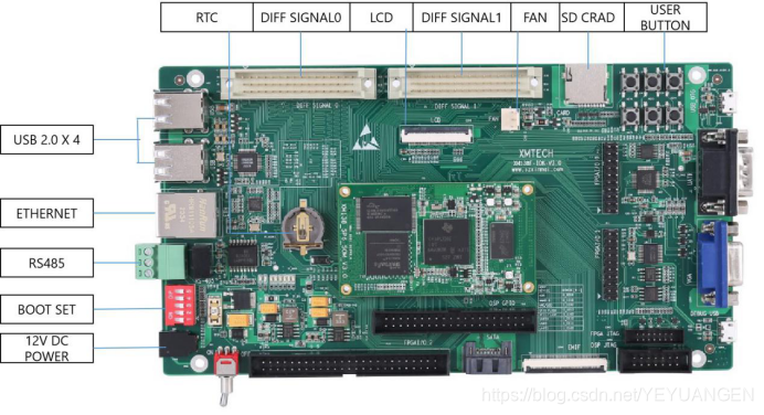
Figure 3: Development board interface diagram
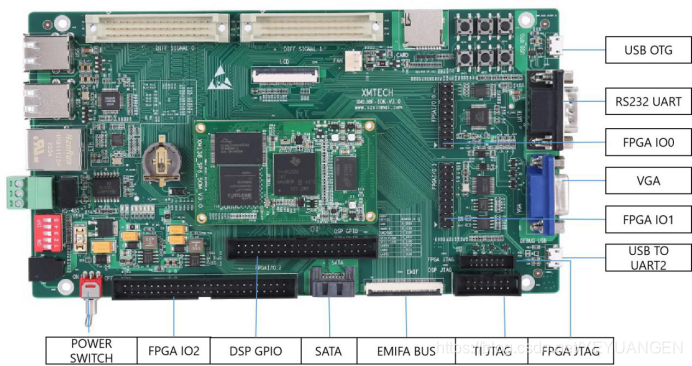
Figure 4: Development board interface diagram