Research on LFMCW Radar Signal Processing Algorithms Based on C6748 DSP + FPGA
With the rapid development of China's economy and the continuous improvement of living standards, automobile usage has become increasingly widespread. However, while cars bring convenience and efficiency to daily life, the frequency of traffic accidents has also risen, posing serious threats to personal safety and property, as well as creating significant risks to social stability. In recent years, with advancements in front-end Monolithic Microwave Integrated Circuits (MMIC) and millimeter-wave devices, millimeter-wave radar technology has matured significantly. Millimeter-wave radars are now installed not only in high-end and mid-range vehicles but also in many entry-level compact cars, greatly promoting the development of smart cities and autonomous driving technologies. This paper introduces the fundamental characteristics of millimeter-wave radar and, based on the Linear Frequency Modulated Continuous Wave (LFMCW) system, analyzes and compares three millimeter-wave radar signal processing methods, discussing their respective advantages, disadvantages, and application scenarios. Finally, building upon theoretical analysis, a millimeter-wave radar system hardware platform is constructed, and a signal processing board based on Field-Programmable Gate Array (FPGA) and Digital Signal Processor (DSP) is designed. The TMS320C6748 DSP is used as the main controller to implement signal processing algorithms and extract valid target information. The main contributions of this thesis are summarized in the following three aspects:
- Analysis of the principles of millimeter-wave radar for range, velocity, and angle measurement, with simulation and comparison of three schemes: multi-period LFMCW, variable-period positive/negative LFMCW, and positive/negative LFMCW combined with a single-frequency signal. By comparing these three algorithms, their respective strengths and weaknesses are evaluated to select the most suitable algorithm for implementation on the DSP hardware.
- Design and implementation of a 24 GHz antenna and radio frequency (RF) solution, including testing of key performance indicators such as antenna layout, transmit power, beamwidth, and maximum detection range.
- Independent design of a DSP-based signal processing module, including associated hardware circuitry and Printed Circuit Board (PCB) layout. A multi-core heterogeneous architecture combining FPGA and DSP is employed to implement the millimeter-wave radar signal processing board. Key signal processing modules such as Finite Impulse Response (FIR) filters, Fast Fourier Transform (FFT), and Kalman filtering are designed and implemented within the DSP. The developed millimeter-wave radar signal processing algorithms are then successfully ported and stably operated on the DSP module to achieve core functionality.
1 Evaluation Board Overview
- Based on TI OMAP-L138 (fixed/floating-point DSP C674x + ARM9) + Xilinx Spartan-6 FPGA processor;
- OMAP-L138 and FPGA connected via uPP, EMIFA, and I2C buses, supporting communication speeds up to 228 MByte/s; OMAP-L138 operates at 456 MHz with computing performance of up to 3648 MIPS and 2746 MFLOPS;
- FPGA compatible with Xilinx Spartan-6 XC6SLX9/16/25/45, offering strong platform scalability;
- The development board exposes abundant peripherals, including high-speed data interfaces such as Gigabit Ethernet, SATA, EMIFA, uPP, and USB 2.0, as well as common interfaces such as GPIO, I2C, RS232, PWM, and McBSP;
- Certified for high and low temperature operation, suitable for harsh working environments;
- DSP + ARM + FPGA tri-core SOM (System-on-Module) measuring 66 mm × 38.6 mm, using industrial-grade B2B connectors to ensure signal integrity;
- Supports bare-metal, SYS/BIOS, and Linux operating systems.
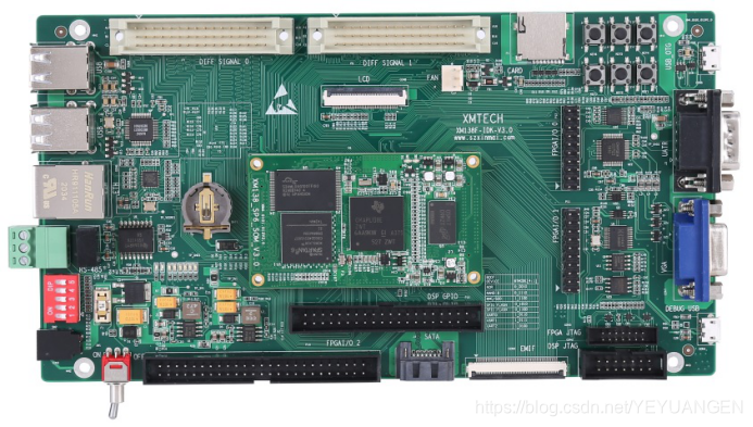
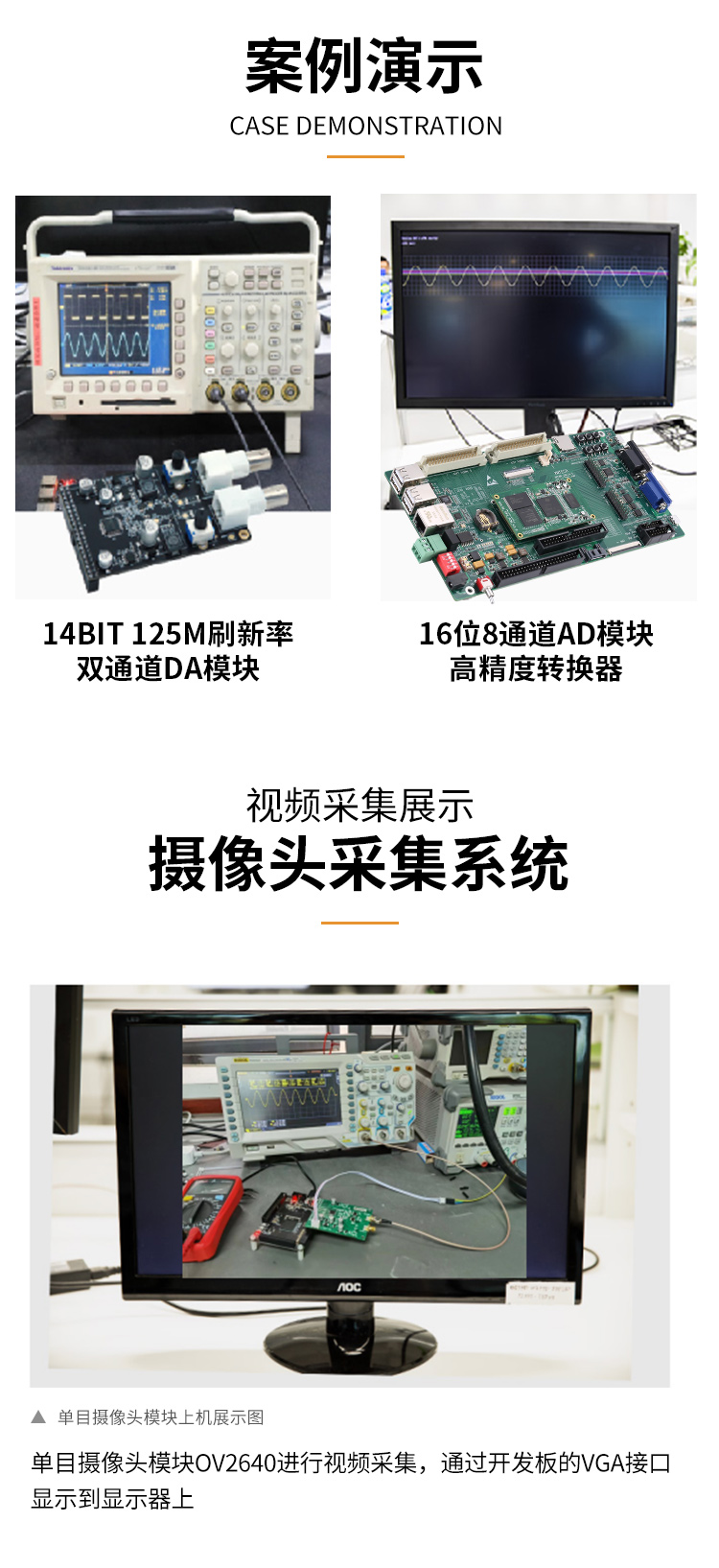
Figure 1 Front and side views of the development board
The XM138F-IDK-V3.0 is a development board designed based on Shenzhen Xinmai’s XM138-SP6-SOM core module. It features a 4-layer PCB design with lead-free immersion gold finish, providing users with a testing platform for the XM138-SP6-SOM core module to rapidly evaluate its overall performance.
The XM138-SP6-SOM exposes all CPU resource signal pins, making secondary development extremely easy. Customers can focus on upper-layer application development, significantly reducing development difficulty and time-to-market, enabling faster product launches and timely capture of market opportunities. In addition to providing rich demo programs, comprehensive development tutorials and full technical support are also offered to assist customers with carrier board design, debugging, and software development.
2 Typical Application Areas
- Data acquisition, processing, and display systems
- Intelligent power systems
- Image processing equipment
- High-precision instruments and meters
- Mid-to-high-end CNC systems
- Communication equipment
- Audio and video data processing
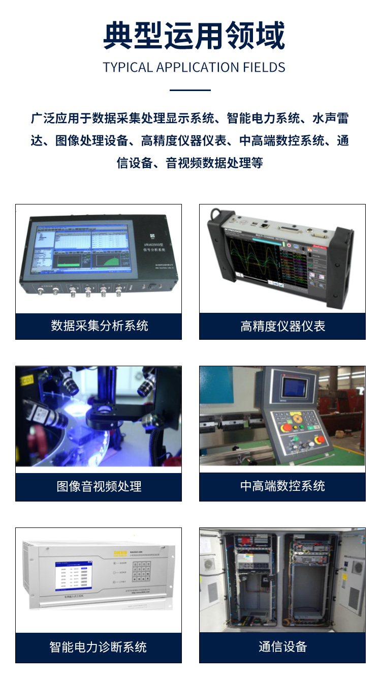
Figure 2 Typical application areas
3 Hardware and Software Specifications
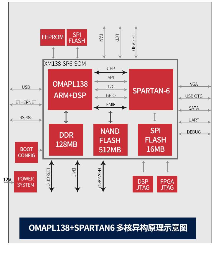
Peripheral resource block diagram of the development board
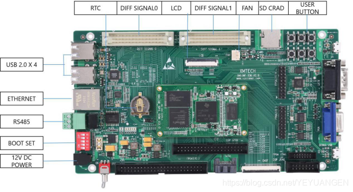
Figure 3 Development board interface diagram
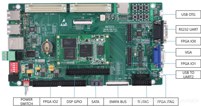
Figure 4 Development board interface diagram