基于TI C6748+ SPARTAN6的多核异构评估板解决方案
Title: Multi-Core Heterogeneous Evaluation Board Solution Based on TI C6748 + Spartan-6
Content:
1 Introduction to the Evaluation Board
- Based on TI TMS320C6748 fixed-point/floating-point DSP C674x + Xilinx Spartan-6 FPGA processor;
- DSP and FPGA connected via uPP, EMIFA, and I2C buses, supporting communication speeds up to 228 MByte/s;
- DSP clock speed of 456 MHz, delivering up to 3648 MIPS and 2746 MFLOPS computational performance;
- FPGA compatible with Xilinx Spartan-6 XC6SLX9/16/25/45, offering strong platform scalability;
- The development board exposes rich peripherals, including Gigabit Ethernet, SATA, EMIFA, uPP, USB 2.0, and other high-speed data transmission interfaces, as well as common interfaces such as GPIO, I2C, RS232, PWM, McBSP, VGA, PMOD, and RS485;
- Passed high and low temperature testing, suitable for harsh operating environments;
- DSP+FPGA dual-core SOM (System-on-Module), measuring 66mm × 38.6mm, using industrial-grade B2B connectors to ensure signal integrity;
- Integrated charge/discharge battery circuit, multiple standard industrial interfaces, supports connection to multi-channel AD, DA, and other modules, offering strong expandability;
- Supports bare-metal and SYS/BIOS operating systems.
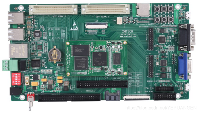
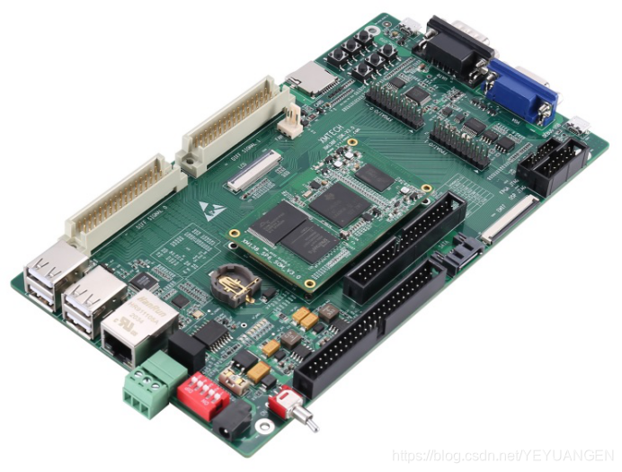
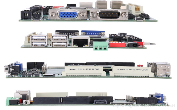
Figure 1 Front and side views of the development board
The XM6748F-IDK-V3.0 is a development board designed based on the Shenzhen Xinming (Xinmai) XM6748F-SOM core module. It features a 4-layer PCB manufactured using lead-free immersion gold process, providing users with a test platform for the XM6748F-SOM core module to rapidly evaluate its overall performance.
The XM6748F-SOM exposes all CPU resource signal pins, making secondary development extremely easy. Customers can focus solely on application-level development, significantly reducing development difficulty and time cost, accelerating time-to-market and enabling early market penetration. In addition to providing abundant demo programs, detailed development tutorials and comprehensive technical support are also offered to assist customers with baseboard design, debugging, and software development.
2 Typical Application Areas
- Data acquisition, processing, and display systems
- Intelligent power systems
- Image processing equipment
- High-precision instruments and meters
- Mid-to-high-end CNC systems
- Communication equipment
- Audio and video data processing
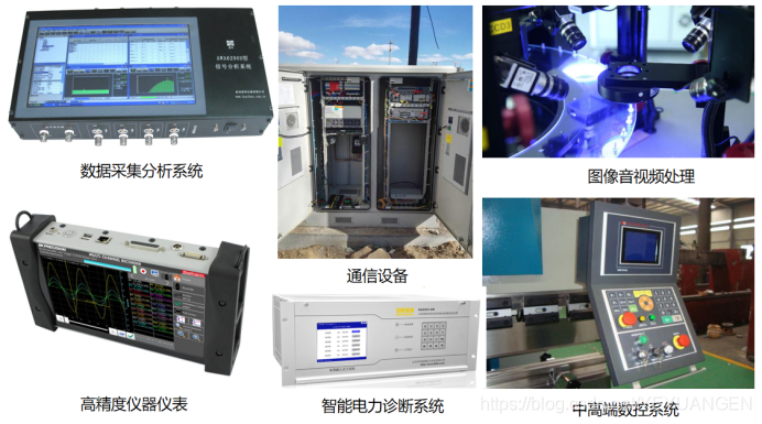
Figure 2 Typical application areas
3 Hardware and Software Specifications
Block diagram of development board peripheral resources
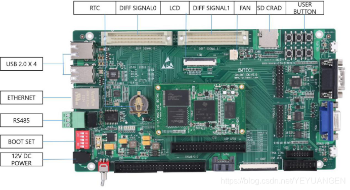
Figure 3 Development board interface diagram
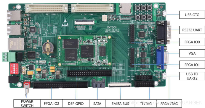
Figure 4 Development board interface diagram
Table 1 Hardware Resources
CPU
TI TMS320C6748, fixed-point/floating-point DSP C674x, 456 MHz
Xilinx Spartan-6 XC6SLX9/16/25/45 FPGA
ROM
TMS320C6748 side: 128/256/512 MByte NAND FLASH
Spartan-6 side: 64 Mbit SPI FLASH
RAM
TMS320C6748 side: 128/256 MByte DDR2
B2B Connector
2×80-pin male B2B, 2×80-pin female B2B, 0.5 mm pitch, total 320 pins
IO
2×25-pin IDC3 header, 2.54 mm pitch, EMIFA expansion signals
2×25-pin IDC3 header, 2.54 mm pitch, FPGA GPIO expansion signals
2×15-pin headers, 2.54 mm pitch, including I2C, McBSP, PWM, FPGA differential IO, and other expansion signals
LED
2× power indicator LEDs (1 on baseboard, 1 on core module)
5× programmable indicator LEDs (3 on baseboard, 2 on core module)
5× programmable indicator LEDs (3 on baseboard, 2 on core module, FPGA side)
KEY
1× system reset button
3× programmable input buttons (including 1 non-maskable interrupt button)
5× programmable indicator LEDs (3 on baseboard, 2 on core module, FPGA side)
JTAG
1× 14-pin TI Rev B JTAG interface, 2.54 mm pitch
1× 14-pin FPGA JTAG interface, 2.00 mm pitch
LCD
1× LCD touch screen interface
BOOT SET
1× 5-bit DIP switch for boot mode selection
SD
1× Micro SD card interface
RTC
1× RC1220 RTC socket, 3V supply
SATA
1× 7-pin SATA hard drive interface
Ethernet
1× RJ45 Ethernet port, 10/100M auto-negotiation
USB
1× Micro USB 2.0 OTG interface
1× USB 1.1 HOST interface
UART
2× RS232 serial ports: UART2 via Micro USB, UART1 via DB9 connector; 4-wire TTL header (TXD, RXD, 3V3, GND) also exposed
SWITCH
1× power toggle switch
POWER
1× 12V 2A DC input via DC417 connector, 4.4 mm outer diameter, 1.65 mm inner diameter
Note: Shenzhen Xinmai XM138F-SOM, XM1808F-SOM, and XM6748F-SOM core modules are pin-to-pin compatible in hardware.
Table 2 Software Resources
DSP Software Support
Bare-metal, SYS/BIOS operating system
CCS Version
CCS 5.5
ISE Version
ISE 14.7
4 Development Resources
(1) Provide core module pin definitions, editable baseboard schematics, editable baseboard PCB, chip datasheets—shortening hardware design cycle;
(2) Provide system flashing images, kernel driver source code, file system source code, and abundant demo programs;
(3) Provide complete platform development packages and getting-started tutorials—saving software integration time and enabling fast onboarding;
(4) Provide rich getting-started tutorials and development examples, including OMAP-L138-to-FPGA communication examples;
(5) Provide detailed DSP+ARM dual-core communication tutorials, effectively solving dual-core development bottlenecks;
(6) Provide GUI development tutorials based on Qt.
Shenzhen Xinmai provides extensive development materials, video tutorials, and Chinese datasheets, creating a new landscape for OMAP-L138 platform development and leading the learning trend for the OMAP-L138 + Spartan-6 DSP+ARM+FPGA tri-core architecture.
Selected development examples are detailed in Appendix A, including:
- Bare-metal development examples for ARM side
- Linux development examples for ARM side
- Bare-metal development examples for DSP side
- SYS/BIOS development examples for DSP side
- SYSLINK-based dual-core development examples
- DSPLINK-based dual-core development examples
- XM_IPC-based dual-core development examples
- PRU assembly development examples
- FPGA-side development examples
5 Electrical Characteristics
Core Module Operating Environment
Table 3
Environmental Parameter
Minimum
Typical
Maximum
Commercial temperature
0°C
/
70°C
Industrial temperature
-40°C
/
85°C
Operating voltage
/
3.3V
/
Power Consumption Test
Table 4
Category
Typical Voltage
Typical Current
Typical Power
Core module
3.3V
74 mA
0.24 W
Entire board
12.01 V
100 mA
1.20 W
Note: Power consumption tests were conducted using the Shenzhen Xinmai XM6748F-IDK-V3 development board.
6 Mechanical Dimensions
Table 5
Core Module
Development Board
PCB Dimensions
66mm × 38.6mm
165mm × 110mm
Number of Mounting Holes
4
12
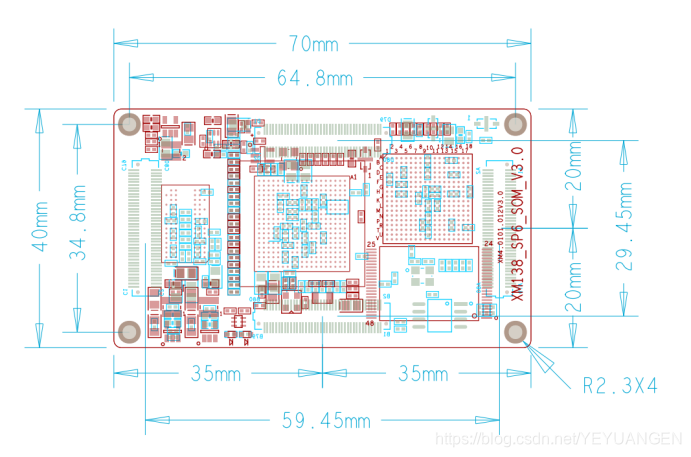
Figure 5 Mechanical Dimensions of the Core Module
7 Product Ordering Models
Table 6
Model
CPU Frequency
NAND FLASH
DDR2
SPI FLASH
FPGA Model
Temperature Grade
SOM-XM6748F-4-4GN1GD2S16-I
456 MHz
512 MB
128 MB
64 Mbit
XC6SLX16
Industrial
SOM-XM6748F-4-4GN2GD2S16-I
456 MHz
512 MB
256 MB
64 Mbit
XC6SLX16
Industrial
SOM-XM6748F-4-4GN1GD2S45-I
456 MHz
512 MB
128 MB
64 Mbit
XC6SLX45
Industrial
SOM-XM6748F-4-4GN2GD2S45-I
456 MHz
512 MB
256 MB
64 Mbit
XC6SLX45
Industrial
Note: Default configuration is SOM-XM6748F-4-4GN1GD2S16-I. Contact sales personnel for other models.
8 Development Board Kit Contents
Table 7
Item
Quantity
XM6748F-IDK-V3 Development Board (with core module)
1 pc
12V/2A Power Adapter
1 unit
Documentation CD
1 set
Micro SD System Card
1 pc
SD Card Reader
1 unit
Straight-through Ethernet Cable
1 piece
Micro USB Data Cable
1 piece
9 Technical Support
(1) Assist with baseboard design and testing to reduce hardware design errors;
(2) Assist in resolving abnormal issues arising from user manual operations;
(3) Assist in product fault diagnosis;
(4) Assist in correctly compiling and running provided source code;
(5) Assist with product secondary development;
(6) Provide long-term after-sales service.
10 Value-Added Services
- Custom baseboard design
- Custom core module design
- Embedded software development
- Joint project development
- Technical training