OMAPL138+SPARTAN6 Core Board and Evaluation Board Review
Last week, I received the OMAPL138 development board from Shenzhen Xinmai Company. My first impression was how small the core board is, about the size of a coin. They used a three-way DC-DC power supply, which results in low power consumption, and all chips are industrial-grade, making it very suitable for our power monitoring equipment.
It's worth noting that they've implemented EMC and ESD protection, so electromagnetic interference in power systems is not a concern. I've been playing with the provided examples for a week, and the QT part is very well done. Just for fun, here are some photos I found online.
- OMAP-L138+FPGA Development Board Introduction The XM138F-IDK-V3 designed by Shenzhen Xinmai is a DSP+ARM+FPGA triple-core high-speed data acquisition and processing development board, suitable for data acquisition and processing in fields such as power, communication, industrial control, medical, and audio/video.
This design utilizes an OMAP-L138+Spartan-6 platform. The OMAP-L138 is a low-power, high-performance floating-point DSP C6748+ARM9 dual-core processor from Texas Instruments (TI), while the Spartan-6 is a flexible and cost-effective FPGA processor from Xilinx, offering excellent platform upgradeability. This design integrates the two chips via OMAP-L138's uPP, EMIF, and other communication interfaces. The DSP and ARM within the OMAP-L138 communicate via DSPLINK/SYSLINK for dual-core communication, realizing a unique, flexible, and powerful DSP+ARM+FPGA triple-core high-speed data acquisition and processing system.
- OMAP-L138+FPGA Development Board Resource Block Diagram
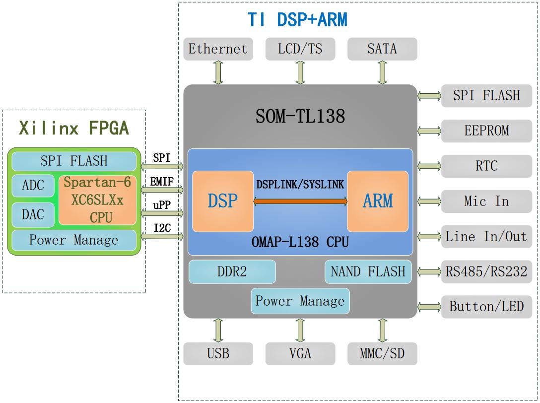
Figure 1 OMAP-L138+FPGA Triple-Core High-Speed Data Acquisition and Processing Resource Block Diagram
Framework Analysis:
The front end, consisting of a Xilinx Spartan-6 XC6SLX9/16/25/45 FPGA, acquires two channels of AD data with a sampling rate of up to 65MHz. The AD data is then transmitted to the OMAP-L138's DSP via the uPP or EMIF bus. After processing by the DSP, the data is sent to the ARM via DSPLINK or SYSLINK dual-core communication components for applications such as application interface development, network forwarding, and SATA hard drive storage. Based on the processing results, the OMAP-L138's DSP or ARM sends logical control commands to the FPGA. The FPGA then controls the on-board DA to achieve logical output, with an update rate of 175MSPS. (1) The high-speed data acquisition front end simultaneously acquires two analog input signals via a Xilinx Spartan-6 XC6SLX9/16/25/45 FPGA. It can perform pre-filtering on AD data, with an AD sampling rate of up to 65MSPS. Another DAC channel can output parallel DA data of arbitrary amplitude and waveform, with an update rate of 175MSPS.
(2) The high-speed data transmission section consists of uPP, EMIF, SPI, and I2C communication buses. Large-throughput AD and DA data can be transmitted at high speed and stability between the DSP and FPGA via the uPP bus; the DSP can perform parallel logical control and medium-throughput data exchange with the FPGA via the EMIF bus; the ARM can perform initialization settings and parameter configuration on the FPGA side via SPI and I2C.
(3) The high-speed data processing section consists of the DSP core and algorithm library. It can perform real-time transformation and processing of time-domain, frequency-domain, amplitude, and other signal parameters for AD and DA data (e.g., FFT transform, FIR filtering).
(4) The DSP+ARM dual-core communication section consists of the DSP core, ARM core, and DSPLINK/SYSLINK dual-core communication components. Data exchange and communication between the DSP and ARM dual cores are achieved through memory sharing.
(5) The data display, storage, and expansion section consists of the ARM core, graphical display, network, and SATA hard drive. The ARM's application interface can display time-domain and frequency-domain waveforms of AD and DA in real-time; it also supports large data storage and remote network communication.
- Xilinx Spartan-6 FPGA High-Speed Data Acquisition Front-End Logic Implementation
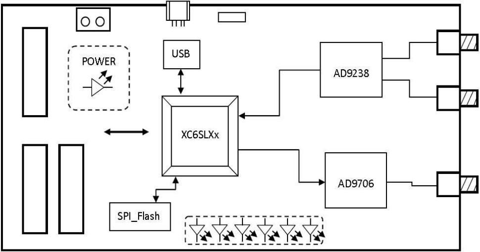
Xilinx Spartan-6 FPGA——XC6SLXx
XC6SLXx is a widely used and cost-effective FPGA platform in the Xilinx Spartan-6 series. It has 324 pins, providing a large number of available I/Os, good platform upgradeability, reasonable hardware cost differences, and smooth scalability. Models like LX9, LX16, LX25, and LX45 can be used according to actual needs. Furthermore, the four CPU models are pin-to-pin compatible.
(1) XC6SLX9: Interface level, capable of interface programming and clock control.
(2) XC6SLX16: Algorithm level, capable of simple algorithm processing.
(3) XC6SLX25: Algorithm level, capable of intermediate algorithm processing.
(4) XC6SLX45: System level, capable of meeting more complex algorithm and system logic processing requirements.
High-Speed ADC——AD9238
The AD9238 is a 12-bit dual-channel A/D converter with the industry's fastest sampling rate, launched by Analog Devices (ADI). It offers selectable voltage input ranges of 1Vp-p and 2Vp-p and is widely used in high-speed data acquisition applications such as power, communication, industrial control, and medical.
The AD9238 comes in three models with sampling rates of 20 MS/s, 40 MS/s, and 65 MS/s, respectively. It not only provides the same excellent dynamic performance as single-channel A/D converters but also offers better crosstalk performance compared to using two single-channel A/D converters. The three models are pin-to-pin compatible, allowing for flexible configuration based on actual needs.
The three AD9238 models consume 180mW, 330mW, and 600mW, respectively, which is only half the power consumption of comparable A/D converters. Packaged in a 64-pin LQFP (only 9mm x 9mm), it is ideal for applications with strict size requirements.
High-Speed DAC——AD9706
The AD9706 is a 12-bit D/A converter with an update rate of 175MSPS, launched by Analog Devices (ADI). It has an output current range of 1mA to 5mA and is widely used in high-speed data output applications such as communication, industrial control, medical, and power.
///All are 175MSPS update rate D/A converters, and these four DAC chips are pin-to-pin compatible, with resolutions of 8/10/12/14 bits respectively. This series of devices is optimized for low power consumption while maintaining excellent dynamic performance, featuring a flexible power supply voltage range (1.7V to 3.6V), making them very suitable for portable and low-power applications. By reducing the full-scale current output, power consumption can be reduced to 15 mW, and in power-saving mode, standby power consumption can be as low as 2.2 mW.
The AD9748/AD9740/AD9742/AD9744 series D/A converters are also pin-to-pin compatible with the above series (LFCSP_VQ package) and are specifically optimized for the transmit signal path in communication systems. Users can select the appropriate device up or down based on performance, resolution, and cost requirements.
- Xilinx Spartan-6 FPGA and TI OMAP-L138 Communication Implementation
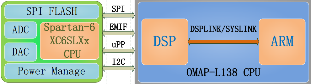 Figure 6 FPGA and OMAP-L138 Communication Principle
High-Speed Communication Bus——uPP
uPP (Universal Parallel Port) is a distinctive high-speed parallel data transfer bus of the OMAP-L138 CPU. It can send and receive data independently or simultaneously, and is commonly used for data transfer with FPGAs and other parallel port devices.
The OMAP-L138's uPP has 2 channels (Channel A and Channel B), with 32 data lines, simple control, flexible configuration, and high data throughput. The uPP clock rate can be up to half of the processor clock rate. For an OMAP-L138 processor running at 456MHz, the theoretical throughput of a single uPP channel can be as high as 228MB/s.
- TI OMAP-L138 DSP and ARM Dual-Core Communication Implementation
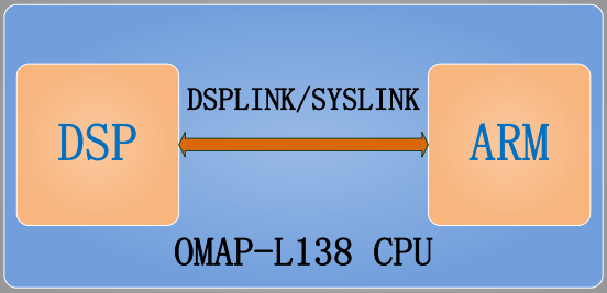 Figure 14 OMAP-L138 DSP+ARM Dual-Core Communication Principle
Basic Principle
TI's official DSPLINK/SYSLINK dual-core communication components provide a set of generic APIs that abstract the physical connection characteristics between ARM and DSP from the application layer, thereby reducing the complexity of user program development. DSPLINK uses the DSP/BIOS operating system, while SYSLINK uses the SYS/BIOS operating system, with SYSLINK being a newer version of the DSPLINK dual-core communication component.
In dual-core communication development between ARM and DSP, the ARM side runs a High-Level Operating System (HLOS), typically Linux, and the DSP side runs a Real-Time Operating System (RTOS), typically DSP/BIOS or SYS/BIOS. Both cores operate at a frequency of 456MHz.
Advantages
(1) The on-chip DSP+ARM architecture of the SOC enables stable dual-core communication, shortening dual-core communication development time.
(2) DSPLINK/SYSLINK dual-core communication components overcome dual-core development bottlenecks, saving R&D costs.
(3) The DSP and ARM architecture on the SOC simplifies hardware design, reducing product power consumption and hardware costs.
1 Evaluation Board Introduction
- Based on TI OMAP-L138 (fixed-point/floating-point DSP C674x+ARM9) + Xilinx Spartan-6 FPGA processor;
- OMAP-L138 FPGA connected via uPP, EMIFA, I2C bus, with communication speeds up to 228MByte/s; OMAP-L138 main frequency 456MHz, with computing power up to 3648MIPS and 2746MFLOPS;
- FPGA compatible with Xilinx Spartan-6 XC6SLX9/16/25/45, strong platform upgrade capability;
- The development board exposes rich peripherals, including Gigabit Ethernet, SATA, EMIFA, uPP, USB 2.0 and other high-speed data transmission interfaces, as well as common interfaces such as GPIO, I2C, RS232, PWM, McBSP;
- Passed high and low-temperature test certification, suitable for various harsh working environments;
- DSP+ARM+FPGA triple-core module, size 66mm*38.6mm, uses industrial-grade B2B connectors to ensure signal integrity;
- Supports bare metal, SYS/BIOS operating system, Linux operating system.
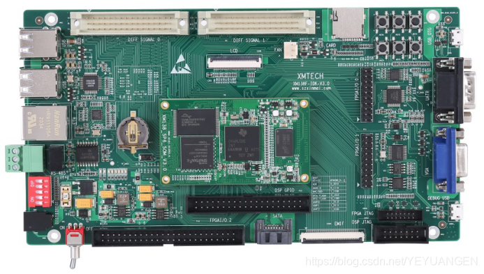
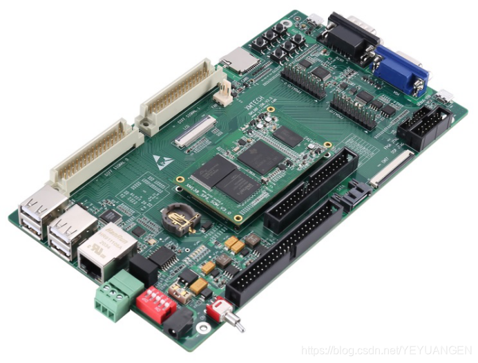
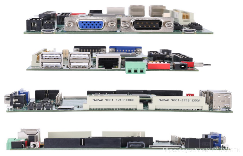
Figure 1 Development Board Front and Side Views
The XM138F-IDK-V3.0 is a development board designed based on Shenzhen Xinmai's XM138-SP6-SOM core module. It features a 4-layer board design with immersion gold lead-free process, providing users with a test platform for the XM138-SP6-SOM core module to quickly evaluate its overall performance.
The XM138-SP6-SOM exposes all CPU resource signal pins, making secondary development extremely easy. Customers only need to focus on the upper-layer application, greatly reducing development difficulty and time costs, allowing products to quickly enter the market and seize market opportunities. It not only provides rich demo programs but also detailed development tutorials, comprehensive technical support, assisting customers with baseboard design, debugging, and software development.
2 Typical Application Areas
- Data Acquisition, Processing, and Display Systems
- Smart Power Systems
- Image Processing Equipment
- High-Precision Instrumentation
- Mid-to-High-End CNC Systems
- Communication Equipment
- Audio and Video Data Processing
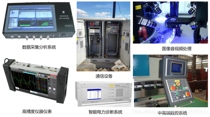
Figure 2 Typical Application Areas
3 Hardware and Software Parameters
Development Board Peripheral Resource Block Diagram
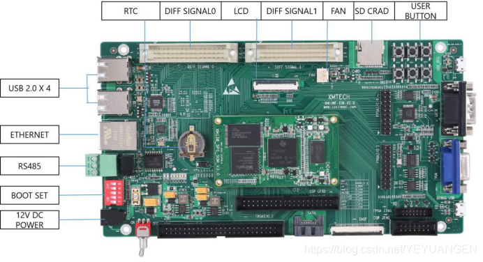
Figure 3 Development Board Interface Diagram
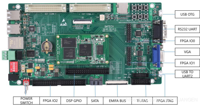
Figure 4 Development Board Interface Diagram
Table 1 Hardware Resources
CPU
TI OMAP-L138, fixed-point/floating-point DSP C674x+ARM9, dual-core main frequency 456MHz
Xilinx Spartan-6 XC6SLX9/16/25/45 FPGA
ROM
OMAP-L138 side: 128/256/512MByte NAND FLASH
Spartan-6 side: 64Mbit SPI FLASH
RAM
OMAP-L138 side: 128/256MByte DDR2
B2B Connector
2x 80pin male B2B, 2x 80pin female B2B, 0.5mm pitch, total 320pin
IO
2x 25pin IDC3 simple box headers, 2.54mm pitch, EMIFA expansion signals
2x 25pin IDC3 simple box headers, 2.54mm pitch, FPGA GPIO expansion signals
2x 15pin headers, 2.54mm pitch, including I2C, McBSP, PWM, FPGA differential IO and other expansion signals
LED
2x Power indicator LEDs (1 on baseboard, 1 on core board)
5x Programmable indicator LEDs (3 on baseboard, 2 on core board)
5x Programmable indicator LEDs (3 on baseboard, 2 on core board, FPGA side)
KEY
1x System reset button
3x Programmable input buttons (including 1 non-maskable interrupt button)
5x Programmable indicator LEDs (3 on baseboard, 2 on core board, FPGA side)
JTAG
1x 14pin TI Rev B JTAG interface, 2.54mm pitch
1x 14pin FPGA JTAG interface, 2.00mm pitch
LCD
1x LCD touchscreen interface
BOOT SET
1x 5bit boot mode selection DIP switch
SD
1x Micro SD card slot
RTC
1x RC1220 RTC socket, 3V voltage
SATA
1x 7pin SATA hard drive interface
Ethernet
1x RJ45 Ethernet port, 10/100M auto-sensing
USB
1x Micro USB 2.0 OTG interface
1x USB 1.1 HOST interface
UART
2x RS232 serial ports, where UART2 uses a Micro USB interface, UART1 uses a DB9 interface, and exposes 4-wire TTL headers (TXD, RXD, 3V3, GND)
SWITCH
1x Power toggle switch
POWER
1x 12V 2A DC input DC417 power interface, outer diameter 4.4mm, inner diameter 1.65mm;
Table 2 Software Resources
ARM Side Software Support
Bare metal, Linux operating system (Linux-3.3, Linux-2.6.37, Linux-2.6.33)
DSP Side Software Support
Bare metal, SYS/BIOS operating system
CCS Version Number
CCS5.5
Graphical Interface Development Tool
Qt
Dual-Core Communication Component Support
SysLink, DSPLink
Software Development Kit Provided
MCSDK, DVSDK
ISE********Version Number
ISE 14.7
Linux********Driver Support
NAND FLASH, DDR2, SPI FLASH, I2C EEPROM, MMC/SD, SATA, USB 2.0 HOST, USB 2.0 OTG, LED, BUTTON, RS232, RS485, UART TL16C754C, CAN MCP2515, AUDIO TLV320AIC3106, Ethernet LAN8710 MII, Ethernet LAN8720 RMII, Ethernet LAN9221 EMIFA, 7in Touch Screen LCD, VGA CS7123, RTC, ADC AD7606, ADC AD7656, ADC ADS8568, DAC AD5724, CMOS Sensor OV2640, Video Decoder TVP5147, USB 3G ZTE MC2716, USB WIFI RTL8188, USB Mouse, USB Keyboard
4 Development Resources
(1) Provides core board pin definitions, editable baseboard schematics, editable baseboard PCBs, chip datasheets, shortening hardware design cycles;
(2) Provides system burning images, kernel driver source code, file system source code, and rich demo programs;
(3) Provides a complete platform development package and introductory tutorials, saving software organization time and making it easy to get started;
(4) Provides rich introductory tutorials and development cases, including OMAP-L138 and FPGA communication examples;
(5) Provides detailed DSP+ARM dual-core communication tutorials, perfectly solving dual-core development bottlenecks;
(6) Provides Qt-based graphical interface development tutorials.
Shenzhen Xinmai has provided a large amount of development resources, video tutorials, and Chinese data manuals, creating a new landscape for OMAP-L138 platform development and leading the OMAP-L138 + Spartan-6 DSP+ARM+FPGA triple-core learning trend.
Some development examples are detailed in Appendix A, mainly including:
- Bare-metal development examples based on ARM
- Linux development examples based on ARM
- Bare-metal development examples based on DSP
- SYS/BIOS development examples based on DSP
- Dual-core development examples based on SYSLINK
- Dual-core development examples based on DSPLINK
- Dual-core development examples based on XM_IPC
- Assembly development examples based on PRU
- FPGA-based development examples
5 Electrical Characteristics
Core Board Operating Environment
Table 3
Environmental Parameters
Min
Typ
Max
Commercial Grade Temperature
0°C
/
70°C
Industrial Grade Temperature
-40°C
/
85°C
Operating Voltage
/
3.3V
/
Power Consumption Test
Table 4
Category
Typical Voltage
Typical Current
Typical Power Consumption
Core Board
3.3V
74mA
0.24W
Full Board
12.01V
100mA
1.20W
Note: Power consumption tests are based on the Shenzhen Xinmai XM138F-IDK-V3 development board.
6 Mechanical Dimensions
Table 5
Core Board
Development Board
PCB Size
66mm*38.6mm
165mm*110mm
Number of Mounting Holes
4
12
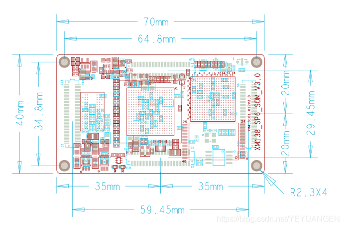
Figure 5 Core Board Mechanical Dimensions
7 Product Ordering Models
Table 6
Model
CPU Frequency
NAND FLASH
DDR2
SPI FLASH
FPGA Model
Temperature Grade
SOM-XM138F-4-4GN1GD2S16-I
456MHz
512MB
128MB
64Mbit
XC6SLX16
Industrial
SOM-XM138F-4-4GN2GD2S16-I
456MHz
512MB
256MB
64Mbit
XC6SLX16
Industrial
SOM-XM138F-4-4GN1GD2S45-I
456MHz
512MB
128MB
64Mbit
XC6SLX45
Industrial
SOM-XM138F-4-4GN2GD2S45-I
456MHz
512MB
256MB
64Mbit
XC6SLX45
Industrial
Note: The standard configuration is SOM-XM138F-4-4GN1GD2S16-I
8 Development Board Kit List
Table 7
Name
Quantity
XM138F-IDK-V3 Development Board (including core board)
1 piece
12V/2A Power Adapter
1 unit
Data CD
1 set
Micro SD System Card
1 unit
SD Card Reader
1 unit
Direct Network Cable
1 cable
Micro USB Data Cable
1 cable
9 Technical Support
(1) Assistance with baseboard design and testing to reduce hardware design errors;
(2) Assistance in resolving abnormal issues encountered when following the user manual;
(3) Assistance in product fault diagnosis;
(4) Assistance in correctly compiling and running the provided source code;
(5) Assistance in product secondary development;
(6) Provision of long-term after-sales service.
10 Value-Added Services
- Mainboard Custom Design
- Core Board Custom Design
- Embedded Software Development
- Project Collaborative Development
- Technical Training