Autonomous Obstacle Avoidance System for UAVs Based on OMAPL138 DSP+ARM+FPGA, Millimeter-Wave Radar, and Monocular Vision Fusion
In recent years, civil small unmanned aerial vehicles (UAVs) have received increasing attention and application, becoming widely used in fields such as express delivery, food delivery, and power line inspection. UAVs equipped with autonomous obstacle avoidance capabilities hold broad application prospects in social production, scientific research, and aerial photography operations. Such systems not only ensure stable flight but also enable UAVs to effectively avoid obstacles during complex missions, reducing damage from collisions and associated secondary hazards. Scholars worldwide have conducted extensive research on UAV autonomous obstacle avoidance. Conventional UAV obstacle avoidance solutions typically rely on pre-existing 3D elevation maps, multi-camera visual sensors, or combinations of multiple sensors. However, existing obstacle avoidance systems generally suffer from drawbacks such as large size, high power consumption, heavy weight, and high cost. Autonomous obstacle avoidance systems that are compact, low-power, lightweight, and low-cost—suitable for installation on small UAVs such as multirotor drones—remain an area requiring further research.
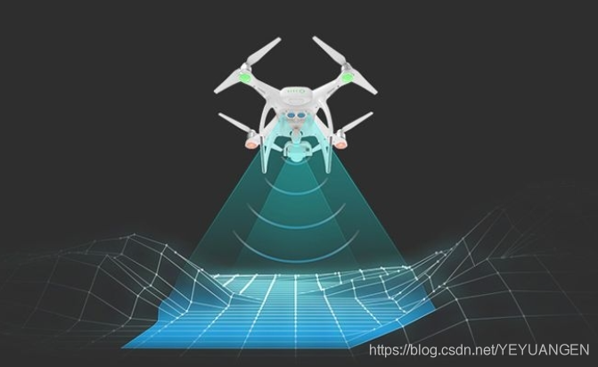
Millimeter-wave radar offers advantages including small size, light weight, and long-distance ranging capability, but it suffers from low accuracy in measuring obstacle azimuth angles. Monocular vision sensors can estimate the azimuth angles of obstacles in the UAV's flight environment and, compared to multi-camera systems, require less computational effort. However, monocular vision performs poorly in measuring obstacle distance. Integrating millimeter-wave radar with a monocular vision sensor on a small UAV enables the acquisition of high-precision obstacle distance and azimuth angle information, achieving complementary strengths between the two sensors. Moreover, the computational load of this solution is low, making it suitable for general embedded microprocessors and ideal for deployment on small UAVs.
Based on this UAV autonomous obstacle avoidance approach, the main research contributions of this paper are as follows:
- A review of the current state of research and development in UAV autonomous obstacle avoidance systems is presented, followed by the proposal of a fusion-based system combining millimeter-wave radar and monocular vision sensors.
- The architecture of millimeter-wave radar and its fundamental principles for obstacle distance measurement are introduced. Methods for applying digital image processing theory to monocular vision-based obstacle angle estimation are investigated. A method for fusing millimeter-wave radar distance measurements with monocular vision angle measurements to achieve 3D obstacle localization is proposed. Additionally, a technique for simplifying complex 3D path planning into 2D path planning is discussed.
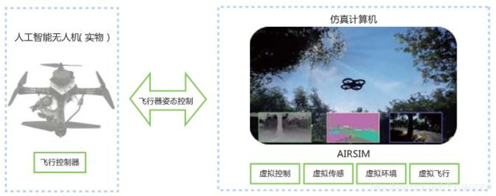
- Based on the Xinmeng OMAPL138 DSP+ARM+FPGA hardware platform, a millimeter-wave radar platform, and the DJI Naza UAV platform, a demonstration system for UAV autonomous obstacle avoidance using millimeter-wave radar and monocular vision fusion was developed. Obstacle avoidance flight experiments were conducted using this system, providing preliminary validation of the feasibility of the proposed fusion approach in UAV autonomous flight.
- Evaluation Board Overview
Based on the TI OMAP-L138 (fixed/floating-point DSP C674x + ARM9) and Xilinx Spartan-6 FPGA processor;
OMAP-L138 and FPGA are connected via uPP, EMIFA, and I2C buses, supporting communication speeds up to 228 MByte/s;
OMAP-L138 operates at a maximum clock frequency of 456 MHz, delivering up to 3648 MIPS and 2746 MFLOPS computational performance;
FPGA supports Xilinx Spartan-6 XC6SLX9/16/25/45, offering strong platform scalability;
The board exposes abundant peripherals, including Gigabit Ethernet, SATA, EMIFA, uPP, USB 2.0, and other high-speed data interfaces, as well as common interfaces such as GPIO, I2C, RS232, PWM, and McBSP;
Certified for high and low temperature operation, suitable for harsh working environments;
The DSP+ARM+FPGA tri-core SOM measures 66mm × 38.6mm and uses industrial-grade B2B connectors to ensure signal integrity;
Supports bare-metal, SYS/BIOS, and Linux operating systems.
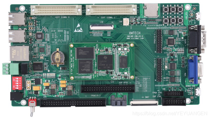
Figure 1 Front and side views of the evaluation board
The XM138F-IDK-V3.0 is a development board designed based on the Shenzhen Xinmeng XM138-SP6-SOM core module, fabricated using a 4-layer lead-free ENIG process. It provides a testing platform for the XM138-SP6-SOM core module, enabling rapid evaluation of its overall performance.
The XM138-SP6-SOM exposes all CPU resource signal pins, making secondary development extremely easy. Customers can focus on upper-layer applications, significantly reducing development difficulty and time-to-market, allowing products to quickly enter the market and gain competitive advantage. In addition to rich demo programs, comprehensive development tutorials and full technical support are provided to assist customers with carrier board design, debugging, and software development.
- Typical Application Areas
Data acquisition, processing, and display systems
Smart power systems
Image processing equipment
High-precision instrumentation
Mid-to-high-end CNC systems
Communication equipment
Audio and video data processing
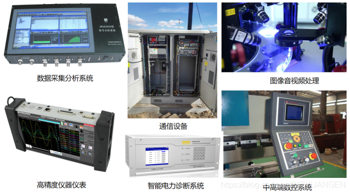
Figure 2 Typical application areas
- Introduction to OMAP-L138 + FPGA Development Board
The XM138F-IDK-V3, designed by Shenzhen Xinmeng, is a high-speed data acquisition and processing development board based on a DSP+ARM+FPGA tri-core architecture, suitable for applications in power systems, communications, industrial control, medical devices, and audio/video processing.
This design employs the OMAP-L138 + Spartan-6 platform. The OMAP-L138 is a low-power, high-performance dual-core processor from Texas Instruments (TI), integrating a floating-point DSP C6748 and an ARM9 core. The Spartan-6 is a Xilinx FPGA processor known for flexible platform scalability and excellent cost-performance ratio. The two chips are interconnected via communication interfaces such as uPP and EMIF on the OMAP-L138, while the internal DSP and ARM cores communicate via DSPLINK/SYSLINK, forming a unique, flexible, and powerful DSP+ARM+FPGA tri-core high-speed data acquisition and processing system.
- Resource Block Diagram of OMAP-L138 + FPGA Development Board
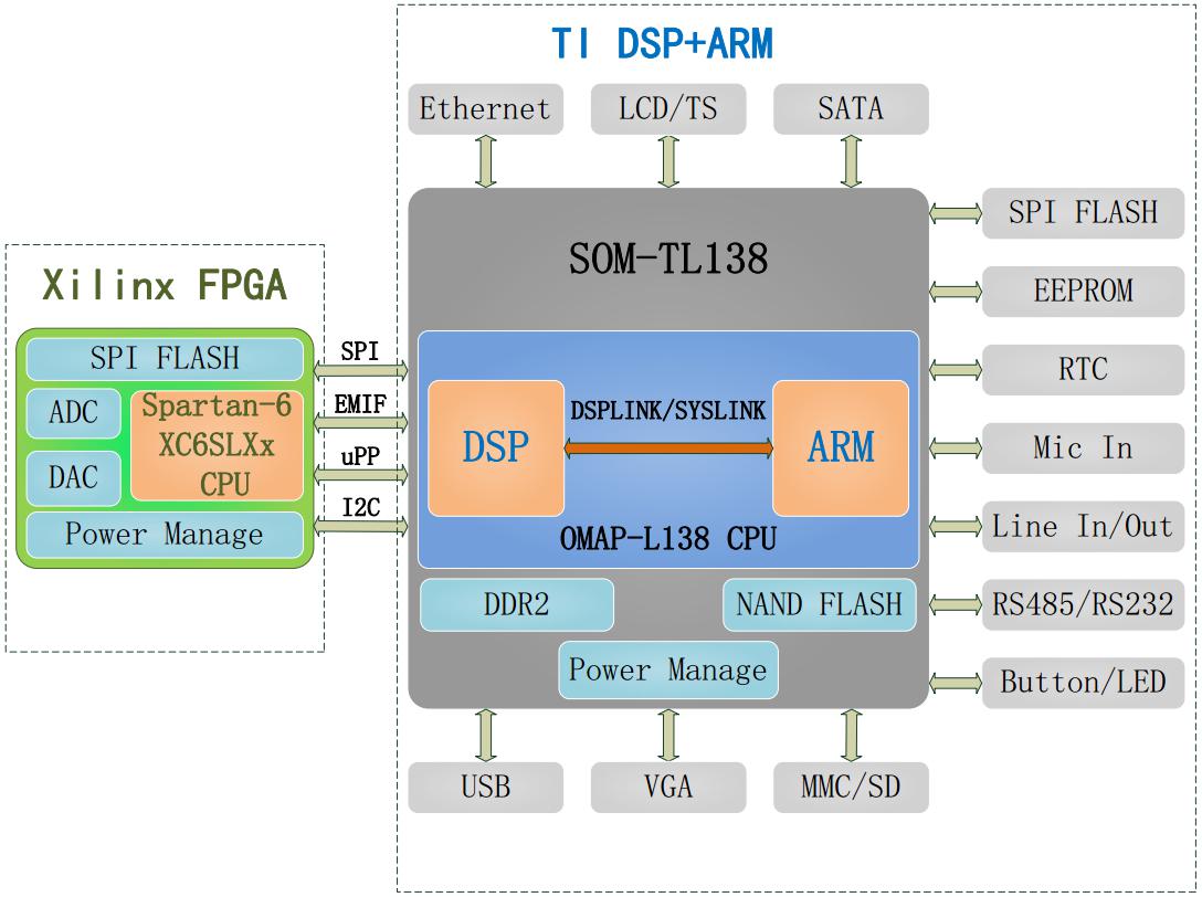
Figure 1 Block diagram of the OMAP-L138 + FPGA tri-core high-speed data acquisition and processing system
System Architecture Description:
- The front end uses a Xilinx Spartan-6 XC6SLX9/16/25/45 FPGA to synchronously acquire two-channel AD data with a maximum sampling rate of 65 MHz. The AD data is transmitted to the OMAP-L138's DSP via the uPP or EMIF bus.
- After processing by the DSP, data is transferred to the ARM via DSPLINK or SYSLINK inter-processor communication components for application interface development, network forwarding, SATA disk storage, and other applications.
- Based on processing results, the OMAP-L138's DSP or ARM sends logic control commands to the FPGA, which drives the onboard DA to generate logic outputs with an update rate of 175 MSPS.
(1) High-speed data acquisition front end: The Xilinx Spartan-6 XC6SLX9/16/25/45 FPGA synchronously acquires two analog input signals and can perform pre-filtering on the AD data, with a maximum sampling rate of 65 MSPS. Another DAC channel outputs parallel DA data with arbitrary amplitude and waveform, updated at 175 MSPS.
(2) High-speed data transmission: Implemented via uPP, EMIF, SPI, and I2C buses. High-throughput AD and DA data are stably transferred between the DSP and FPGA via the uPP bus. The DSP controls FPGA logic and performs medium-throughput data exchange via the EMIF bus. The ARM configures and initializes the FPGA via SPI and I2C.
(3) High-speed data processing: Composed of the DSP core and algorithm libraries, enabling real-time signal processing such as FFT and FIR filtering for time-domain, frequency-domain, and amplitude analysis of AD and DA data.
(4) DSP+ARM dual-core communication: Composed of the DSP core, ARM core, and DSPLINK/SYSLINK inter-processor communication components. Data exchange between the DSP and ARM is achieved via shared memory.
(5) Data display and storage expansion: Composed of the ARM core, graphics display, network, and SATA disk. The ARM-based application interface enables real-time display of time-domain and frequency-domain waveforms of AD and DA signals, as well as large-scale data storage and remote network communication.
- Xilinx Spartan-6 FPGA High-Speed Data Acquisition Front-End Logic Implementation
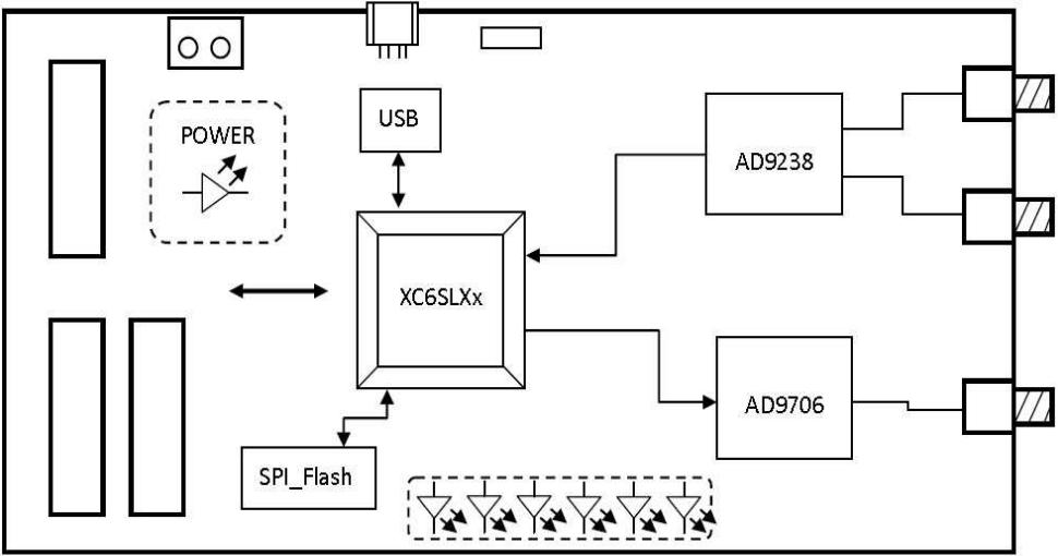
Xilinx Spartan-6 FPGA — XC6SLXx
The XC6SLXx is a widely used, cost-effective FPGA platform from the Xilinx Spartan-6 series, featuring 324 pins, abundant available I/Os, good platform scalability, reasonable cost differences across variants, and smooth scalability. Depending on application needs, models such as LX9, LX16, LX25, and LX45 can be selected. Additionally, these four CPU models are pin-to-pin compatible.
(1) XC6SLX9: Interface-level, capable of interface programming and clock control.
(2) XC6SLX16: Algorithm-level, suitable for simple algorithm processing.
(3) XC6SLX25: Algorithm-level, capable of intermediate-level algorithm processing.
(4) XC6SLX45: System-level, meeting requirements for complex algorithms and system logic processing.
High-Speed ADC — AD9238
The AD9238 is a 12-bit dual-channel A/D converter from Analog Devices (ADI), offering the industry’s fastest sampling rates. It supports selectable input voltage ranges of 1 Vp-p and 2 Vp-p and is widely used in high-speed data acquisition applications in power, communications, industrial control, and medical systems.
The AD9238 comes in three variants with sampling rates of 20 MS/s, 40 MS/s, and 65 MS/s. It delivers dynamic performance comparable to single-channel ADCs and offers better crosstalk immunity than using two separate single-channel ADCs. The three variants are pin-to-pin compatible, enabling flexible configuration based on requirements.
The power consumption of the three AD9238 variants is 180 mW, 330 mW, and 600 mW, respectively—about half that of comparable ADCs. Packaged in a 64-pin LQFP (9 mm × 9 mm), it is ideal for space-constrained applications.
High-Speed DAC — AD9706
The AD9706 is a 12-bit D/A converter from Analog Devices with a 175 MSPS update rate and output current range of 1 mA to 5 mA, widely used in high-speed data output applications in communications, industrial control, medical, and power systems.
/// All are 175 MSPS update-rate D/A converters, pin-to-pin compatible, with resolutions of 8, 10, 12, and 14 bits. These devices are optimized for low power while maintaining excellent dynamic performance, support flexible supply voltage ranges (1.7 V to 3.6 V), and are ideal for portable and low-power applications. Power consumption can be reduced to 15 mW by lowering full-scale output current, and standby power in power-down mode can be as low as 2.2 mW.
The AD9748/AD9740/AD9742/AD9744 series D/A converters are also pin-to-pin compatible (in LFCSP_VQ package) and optimized for transmit signal paths in communication systems. Users can select suitable devices based on performance, resolution, and cost requirements.
- Implementation of Communication Between Xilinx Spartan-6 FPGA and TI OMAP-L138
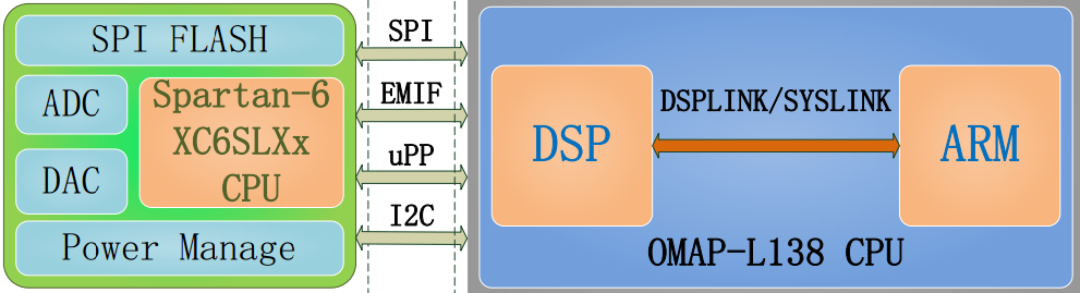
Figure 6 FPGA-OMAP-L138 Communication Principle
High-Speed Communication Bus — uPP
The uPP (Universal Parallel Port) is a distinctive high-speed parallel data transfer interface on the OMAP-L138 CPU. It supports independent or simultaneous data transmission and reception, commonly used for data exchange with FPGAs and other parallel-interface devices.
The OMAP-L138 uPP features two channels (Channel A and Channel B), 32 data lines, simple control, flexible configuration, and high data throughput. The uPP clock rate can reach up to half the processor clock rate. For the OMAP-L138 running at 456 MHz, the theoretical single-channel throughput can reach up to 228 MB/s.
- Implementation of DSP and ARM Dual-Core Communication on TI OMAP-L138
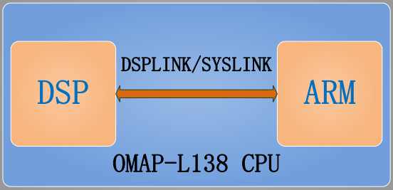
Figure 14 OMAP-L138 DSP+ARM Dual-Core Communication Principle
Basic Principle
TI's official DSPLINK/SYSLINK dual-core communication components provide a set of generic APIs that abstract the physical connection characteristics between ARM and DSP at the application layer, reducing development complexity. DSPLINK operates with the DSP/BIOS OS, while SYSLINK uses the SYS/BIOS OS; SYSLINK is the newer version of the DSPLINK dual-core communication component.
In dual-core development, the ARM runs a high-level operating system (HLOS), typically Linux, while the DSP runs a real-time operating system (RTOS), usually DSP/BIOS or SYS/BIOS. Both cores operate at 456 MHz.
Advantages
(1) The on-chip DSP+ARM architecture enables stable dual-core communication, significantly reducing development time.
(2) The DSPLINK/SYSLINK components overcome dual-core development bottlenecks, reducing R&D costs.
(3) The integration of DSP and ARM on a single SOC simplifies hardware design, lowering product power consumption and hardware costs.