TI DSP TMS320C66x (1) Hardware Overview
Table of Contents
- Overview
- C66x Processor Core
- C66x Pipeline Architecture
Overview
The C66x DSP represents the latest generation of fixed- and floating-point DSPs, featuring four multipliers designed to perform single-precision floating-point operations. The C66x DSP core can simultaneously execute up to eight floating-point multiplication operations. Combined with a maximum clock frequency of up to 1.4 GHz, this delivers exceptional floating-point processing performance. By integrating multiple C66x DSP cores with other processing elements, highly scalable multicore System-on-Chip (SoC) devices with mid-to-high performance can be created. This article uses the TMS320C6678 as an example to introduce the C66x core.
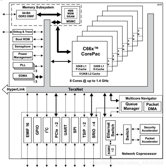
The TMS320C6678 integrates eight C66x cores, each operating at a maximum core frequency of 1.4 GHz, delivering a theoretical processing performance of 179.2 (22.4×8) GFLOPS and 358.4 (44.8×8) GMACS. Each processor includes a multi-level memory hierarchy: L1P, L1D, and L2 SRAM within the C66x core, and shared multi-core memory in the form of MSM SRAM. The processor also features several shared multicore peripherals such as a Multicore Navigator, Network Coprocessor, Packet Accelerator, Semaphore module, and PLL, along with multiple external interfaces including SRIO, PCIe, and EMIF. The architecture of the C6678 is shown in the figure below:
C66x Processor Core
The C66x core is the central processing unit of the C6678, responsible for executing high-performance computing tasks.
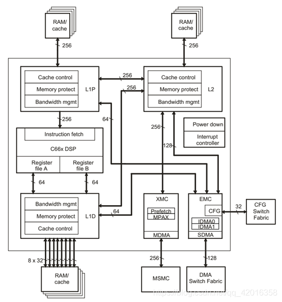
The C66x core consists of the following components: C66x DSP, Level 1 Program Memory Controller (L1P), Level 1 Data Memory Controller (L1D), Level 2 Memory Controller (L2), External Memory Controller (EMC), Extended Memory Controller (XMC), Bandwidth Manager (BWM), and Power and Debug Controller (PDC). The core architecture is illustrated below:
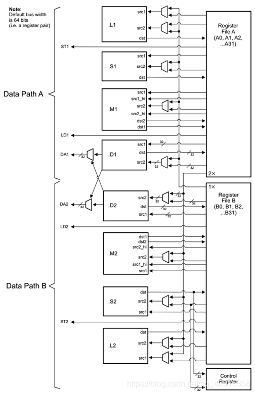
The C66x DSP comprises eight functional units, two register files, and two data paths, as shown in the figure below. The two register files contain a total of 64 registers, divided into two groups—A and B—each consisting of 32 32-bit registers. General-purpose registers can store data or serve as address pointers. Supported data types include 8-bit packed data, 16-bit packed data, 32-bit data, 40-bit data, and 64-bit data. Multiplication operations support 128-bit data.
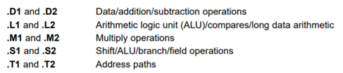
The eight functional units (.L1, .S1, .M1, .D1, .L2, .S2, .M2, .D2) can each execute one instruction per clock cycle. The .S units handle typical shift, branch, and comparison operations; the .L units perform standard arithmetic and logical operations; all multiplication instructions are executed in the .M units (each .M unit contains 16 sets of 16×16-bit multipliers, capable of performing one single-precision floating-point multiplication per cycle, or one double-precision floating-point multiplication in four cycles). The .D units primarily handle loading data from memory into the register file and storing results from the register file back to memory.
C66x Pipeline Architecture
Processor pipelining was first introduced by Intel in the 486 chip. In a CPU, instruction execution is divided into several distinct functional stages. These stages are implemented using separate circuit units that form an instruction processing pipeline. An instruction (e.g., x86) is broken down into multiple steps, each handled by a corresponding circuit unit. This allows the CPU to complete one instruction per clock cycle, significantly improving processing speed.
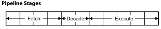
The C66x DSP pipeline is divided into three main stages: Fetch, Decode, and Execute. The detailed pipeline structure for each stage is shown below:
Stage
Pipeline Name
Description
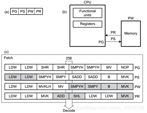
Fetch
PG
Program address generation: Generates program addresses
PS
Program address send: Sends program addresses
PW
Program (memory) access ready wait: Waits for memory response
PR
Program fetch packet receive: Receives instruction packets from memory
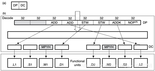
Decode
DP
Instruction dispatch: Routes instructions to appropriate functional units
DC
Instruction decode: Decodes instructions within the assigned functional units
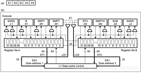
Execute
E1
Instruction execution; different instructions have different execution pipeline steps
...
E5
- Fetch stage pipeline diagram:
- Decode stage pipeline diagram:
- Execute stage pipeline diagram: